
 German
 Japanese
 Portuguese
 Korea
Korea
 Mexico
 Dutch
Dutch


Texas Instruments
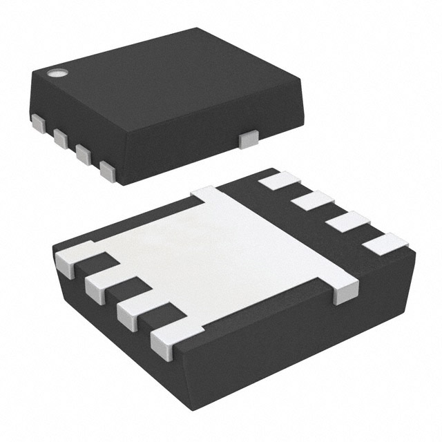
CSD16410Q5A

Why Choose Us?
Professional Platform
B2B & B2C purchasingDelivery at full speed
1-2 days deliveryWide variety
Original manufacturers365 days guarantee
Responsible quality
.png)


Tech Specifications
CSD16410Q5A Description
CSD16410Q5A is a high performance, low power, 16-channel Smart Switch from Texas Instruments. It is designed to provide efficient power distribution and load switching for a wide range of applications.
Description:
The CSD16410Q5A is a highly integrated, 16-channel Smart Switch that offers high efficiency and low power consumption. It is designed to provide efficient power distribution and load switching for a wide range of applications, including automotive, industrial, and consumer electronics.
Features:
- 16 channels of load switching with independent control
- Wide input voltage range of 2.7V to 18V
- Low quiescent current of 1.5uA in standby mode
- High efficiency up to 94%
- Integrated gate drivers for external MOSFETs
- Over-current protection and short-circuit protection
- Thermal shutdown and over-voltage protection
- I2C and PWM control interfaces
- Small package size of 7x7mm QFN
Applications:
- Automotive applications such as infotainment systems, lighting control, and power distribution
- Industrial applications such as motor control, power distribution, and load switching
- Consumer electronics such as power supplies, battery charging, and load switching
- Telecommunications equipment such as power distribution and load switching
- Medical equipment such as power supplies and load switching
In summary, the CSD16410Q5A is a highly integrated, efficient, and low power Smart Switch that offers a wide range of features and is suitable for a variety of applications. Its small package size and low quiescent current make it an ideal choice for space-constrained and power-sensitive applications.
FAQ
Not available to buy online? Want the lower wholesale price? Please Send RFQ to get best price, we will respond immediately


.png?x-oss-process=image/format,webp/resize,h_32)


