Texas Instruments_CSD25301W1015

Texas Instruments
CSD25301W1015  
Single FETs, MOSFETs

Texas Instruments
CSD25301W1015
278-CSD25301W1015
Ersa
Texas Instruments-CSD25301W1015-datasheets-10621251.pdf
MOSFET P-CH 20V 2.2A 6DSBGA
In Stock : 12711

Not available to buy online? Want the lower wholesale price? Please Send RFQ to get best price, we will respond immediately

QUICK RFQ
ADD TO RFQ LIST
ersa FreeSample ersa flow
ISO9001
Quality Policy
ISO45001
ISO14001

CSD25301W1015 Description
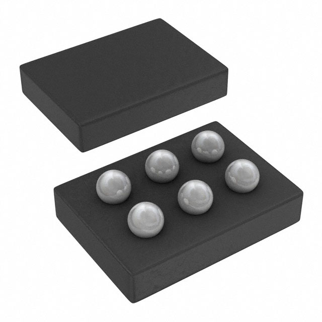
Tape & Reel (TR) provides mechanical support to the IC chip to ensure proper alignment and prevent damage due to vibration or shock. The Single FETs, MOSFETs that the CSD25301W1015 belongs to can be classified under the Discrete Semiconductors. CSD25301W1015 is used in a wide range of electronic devices, including computers, smartphones, televisions, cars, medical devices, and many others. CSD25301W1015 provides the computational power and functionality that enable these devices to perform their intended tasks. a vital part of the supply chain ecosystem. They convert raw materials or components into finished products, ensuring their availability for consumers or other businesses. Texas Instruments plays a crucial role in ensuring the smooth flow of goods and meeting market demand. Texas Instruments is responsible for ensuring the quality and safety of the products they produce. They implement quality control measures to meet industry standards and regulatory requirements. By maintaining high-quality standards, Texas Instruments builds trust with consumers and enhances the overall reputation of their products.

Tech Specifications

FET Type
Input Capacitance (Ciss) (Max) @ Vds
Gate Charge (Qg) (Max) @ Vgs
Product Status
Supplier Device Package
Drain to Source Voltage (Vdss)
Power Dissipation (Max)
Package / Case
Technology
REACH Status
Mfr
Vgs (Max)
RoHS Status
Moisture Sensitivity Level (MSL)
Operating Temperature
FET Feature
ECCN
Mounting Type
Rds On (Max) @ Id, Vgs
Vgs(th) (Max) @ Id
Series
Current - Continuous Drain (Id) @ 25°C
Drive Voltage (Max Rds On, Min Rds On)
HTSUS
Package
Base Product Number
Typical Input Capacitance @ Vds (pF)
Category
Configuration
PCB changed
Typical Turn-Off Delay Time (ns)
Number of Elements per Chip
ECCN (US)
Typical Rise Time (ns)
PPAP
Maximum Power Dissipation (mW)
Channel Mode
Typical Turn-On Delay Time (ns)
Automotive
Minimum Operating Temperature (°C)
Maximum Operating Temperature (°C)
Supplier Package
Typical Fall Time (ns)
Process Technology
Package Height
Typical Gate to Source Charge (nC)
Channel Type
Typical Drain Source Resistance @ 25°C (mOhm)
EU RoHS
Maximum Continuous Drain Current (A)
Maximum Gate Source Voltage (V)
Maximum Drain Source Voltage (V)
Maximum Drain Source Resistance (mOhm)
Package Length
Standard Package Name
Typical Reverse Recovery Charge (nC)
Pin Count
Mounting
Typical Output Capacitance (pF)
Lead Shape
Part Status
Typical Gate to Drain Charge (nC)
SVHC
Maximum Gate Threshold Voltage (V)
Package Width
Typical Gate Charge @ Vgs (nC)

CSD25301W1015 Documents

Download datasheets and manufacturer documentation for CSD25301W1015

Ersa CSD25301W1015      
Ersa DSBGA-6L Carrier Tape Change 28/Oct/2013       Carrier Tape 28/Aug/2018      
Ersa Multiple Devices 20/Feb/2014      
Ersa CSD25301W1015      
Ersa DSBGA/Usip 14/Sep/2016       DSBGA/uSIP 22/Jun/2016      

Shopping Guide

Payment Methods
Payment Methods include Prepayment TT (bank transfer), Western Union, and PayPal. Customers are responsible for shipping costs, bank charges, customs duties and taxes.
Shipping Rate
Shipments are made once a day around 5pm, excluding Sundays. Once shipped, the estimated delivery time is usually 5-7 business days, depending on the courier you choose.
Delivery Methods
Provide DHL, FedEx, UPS, EMS, SF Express and Registered Airmail International Delivery Service