
Texas Instruments
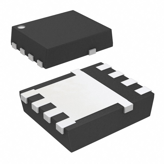
CSD17507Q5A
Single FETs, MOSFETs


- 1+
- $0.71059
- $0.71
- 10+
- $0.59003
- $5.9
- 30+
- $0.52975
- $15.89
- 100+
- $0.47064
- $47.06
- 500+
- $0.43470
- $217.35
- 1000+
- $0.41615
- $416.15

.png?x-oss-process=image/format,webp/resize,p_30)


CSD17507Q5A Description
The Texas Instruments CSD17507Q5A is a highly-integrated, high-voltage gate driver with advanced features designed to drive power switches in a wide range of applications. Here's a brief description of the model, its features, and potential applications:
Description:
The CSD17507Q5A is a member of Texas Instruments' portfolio of gate driver ICs. It is designed to provide precise control and protection for high-voltage power switches, making it suitable for various power conversion applications.
Features:
-
High-Voltage Operation: The CSD17507Q5A is designed to operate with high-voltage power switches, making it suitable for applications that require high-voltage switching.
-
Integrated Protection Features: The device includes built-in protection features such as overcurrent protection, overvoltage protection, and undervoltage lockout to ensure the safe operation of the power switches.
-
High-Side and Low-Side Drive Capability: The CSD17507Q5A can drive both high-side and low-side power switches, providing flexibility in system design.
-
Spread Spectrum Frequency Modulation: This feature helps reduce electromagnetic interference (EMI) and improves system efficiency.
-
Desaturation Protection: The device monitors the current flowing through the power switches and can take corrective action if the current exceeds safe levels.
-
Communication Interface: The CSD17507Q5A typically includes a communication interface (such as SPI) for configuration and monitoring of the device.
-
Small Package Size: Despite its high-voltage capabilities, the CSD17507Q5A is available in a small package, which can help save space on the printed circuit board (PCB).
Applications:
-
Automotive Applications: The device can be used in various automotive applications, such as electric vehicle (EV) traction inverters, battery management systems, and DC-DC converters.
-
Industrial Control Systems: In industrial settings, the CSD17507Q5A can be used to drive power switches in motor control applications, power supplies, and renewable energy systems.
-
Power Supplies: The device is suitable for use in high-voltage power supply designs, including isolated and non-isolated converters.
-
Renewable Energy Systems: In solar power systems and wind turbines, the CSD17507Q5A can be used to drive power switches in the power conversion stages.
-
UPS Systems: Uninterruptible power supply (UPS) systems can benefit from the high-voltage gate driving capabilities of the CSD17507Q5A.
-
Battery Chargers: In high-voltage battery charging systems, the CSD17507Q5A can be used to drive the power switches in the charging circuitry.
When using the CSD17507Q5A or any other high-voltage gate driver, it's essential to carefully review the datasheet and design guidelines to ensure proper operation and to take full advantage of the device's features.
Tech Specifications
CSD17507Q5A Documents
Download datasheets and manufacturer documentation for CSD17507Q5A
 Function Diagram
  CSD17507Q5A Symbol & Footprint by SnapMagic
  Power Management Guide 2018 (Rev. R)
  CSD17507Q5A TINA-TI Spice Model CSD17507Q5A PSpice Model (Rev. A)
 Shopping Guide


.png?x-oss-process=image/format,webp/resize,h_32)


