
 German
 Japanese
 Portuguese
 Korea
Korea
 Mexico
 Dutch
Dutch


Texas Instruments
CSD23202W10T

Why Choose Us?
Professional Platform
B2B & B2C purchasingDelivery at full speed
1-2 days deliveryWide variety
Original manufacturers365 days guarantee
Responsible quality
.png)


Tech Specifications
CSD23202W10T Description
CSD23202W10T Description
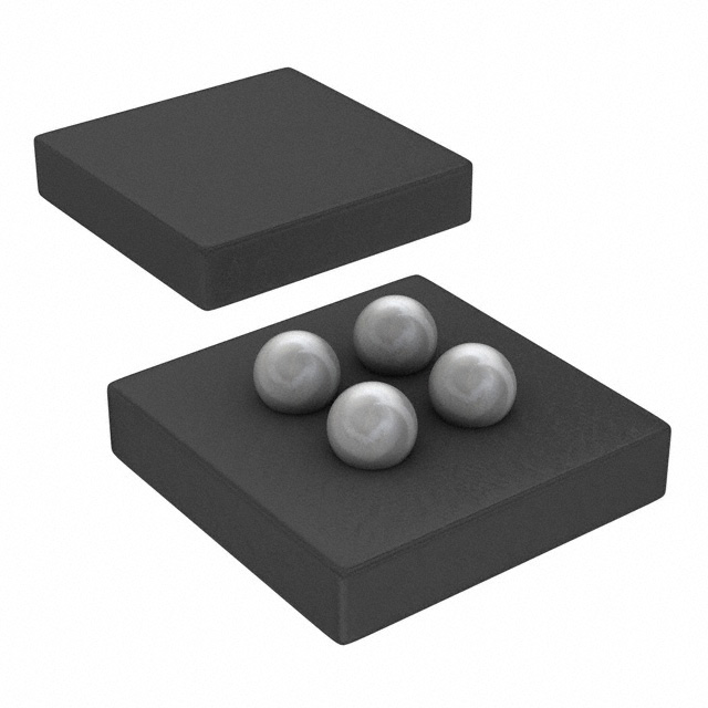
The CSD23202W10T from Texas Instruments is a high-performance P-Channel MOSFET from the NexFET™ series, designed for efficient power management in compact, surface-mount applications. With a 12V drain-to-source voltage (Vdss) and 2.2A continuous drain current (Id), this MOSFET is optimized for low-voltage, high-efficiency switching. Its 4DSBGA package ensures minimal footprint, making it ideal for space-constrained designs. The device features a low on-resistance (Rds On) of 53mOhm @ 500mA, 4.5V, reducing conduction losses and improving thermal performance.
CSD23202W10T Features
- Low Gate Charge (Qg): 3.8 nC @ 4.5V ensures fast switching and reduced drive losses.
- Low Input Capacitance (Ciss): 512 pF @ 6V minimizes switching delays.
- Optimized Drive Voltage: Operates efficiently at 1.5V to 4.5V, compatible with low-voltage logic.
- Robust Thermal Performance: 1W power dissipation (Ta) ensures reliability under load.
- Industry-Leading Packaging: Tape & Reel (TR) for automated assembly, MSL 1 (Unlimited) for moisture resistance.
- Compliance: ROHS3, REACH Unaffected, ECCN EAR99, meeting global environmental standards.
CSD23202W10T Applications
- Portable Electronics: Ideal for battery-powered devices due to low Rds On and efficient power handling.
- Load Switching: Suitable for power distribution in IoT modules, wearables, and smartphones.
- DC-DC Converters: Enhances efficiency in synchronous buck/boost topologies.
- Motor Control: Provides reliable switching in low-power motor drivers.
Conclusion of CSD23202W10T
The CSD23202W10T stands out for its low Rds On, fast switching, and compact form factor, making it a superior choice for modern power management applications. Its NexFET™ technology ensures high efficiency, while compliance with ROHS3 and REACH underscores its environmental safety. Whether in portable gadgets, power converters, or motor controls, this MOSFET delivers performance, reliability, and space savings—key for next-gen electronics.
FAQ
Not available to buy online? Want the lower wholesale price? Please Send RFQ to get best price, we will respond immediately


.png?x-oss-process=image/format,webp/resize,h_32)


