
 German
 Japanese
 Portuguese
 Korea
Korea
 Mexico
 Dutch
Dutch


Texas Instruments
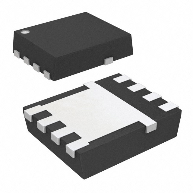
CSD18563Q5A

Why Choose Us?
Professional Platform
B2B & B2C purchasingDelivery at full speed
1-2 days deliveryWide variety
Original manufacturers365 days guarantee
Responsible quality
.png)


Tech Specifications
CSD18563Q5A Description
The CSD18563Q5A is a high-performance, smart power switch from Texas Instruments (TI). It is designed to provide efficient and reliable power management in various applications, including industrial, automotive, and consumer electronics.
Description:
The CSD18563Q5A is a monolithic, synchronous, current-mode, step-down power management switch that integrates a high-voltage power MOSFET and a gate driver. It features a wide input voltage range, low quiescent current, and high efficiency, making it suitable for a wide range of power management applications.
Features:
- Wide input voltage range: The CSD18563Q5A can operate with input voltages from 4V to 60V, making it suitable for various power supply sources.
- High efficiency: The device offers high efficiency of up to 96%, which helps reduce power dissipation and improve overall system performance.
- Low quiescent current: The CSD18563Q5A has a low quiescent current of just 3.5µA in burst mode, which helps extend the battery life in portable applications.
- Synchronous rectification: The device uses synchronous rectification to minimize power losses and improve efficiency.
- Integrated gate driver: The CSD18563Q5A includes an integrated gate driver for the high-voltage power MOSFET, simplifying the design and reducing component count.
- Programmable soft-start: The soft-start feature allows for controlled inrush current during power-up, reducing stress on the power supply and components.
- Protection features: The device offers various protection features, including over-current protection, over-voltage protection, and thermal shutdown.
Applications:
- Industrial control systems: The CSD18563Q5A can be used in industrial control systems for motor control, power supply regulation, and battery management.
- Automotive applications: The device is suitable for automotive applications, such as infotainment systems, lighting control, and battery management systems.
- Consumer electronics: The CSD18563Q5A can be used in portable devices, like smartphones, laptops, and tablets, for efficient power management and battery charging.
- LED lighting: The device can be used in LED lighting applications for efficient power conversion and dimming control.
- Medical equipment: The CSD18563Q5A can be used in medical equipment, such as portable medical devices and diagnostic equipment, for reliable power management.
In summary, the CSD18563Q5A from Texas Instruments is a versatile and efficient power management switch that offers a wide input voltage range, high efficiency, and various protection features. It is suitable for a wide range of applications, including industrial control systems, automotive applications, consumer electronics, LED lighting, and medical equipment.
FAQ
| Quantity | Unit Price | Ext. Price |
|---|---|---|
| 10+ | $0.69943 | $6.99 |
| 30+ | $0.61372 | $18.41 |
| 100+ | $0.54172 | $54.17 |
| 500+ | $0.51943 | $259.71 |
| 1000+ | $0.50572 | $505.72 |
Not available to buy online? Want the lower wholesale price? Please Send RFQ to get best price, we will respond immediately


.png?x-oss-process=image/format,webp/resize,h_32)


