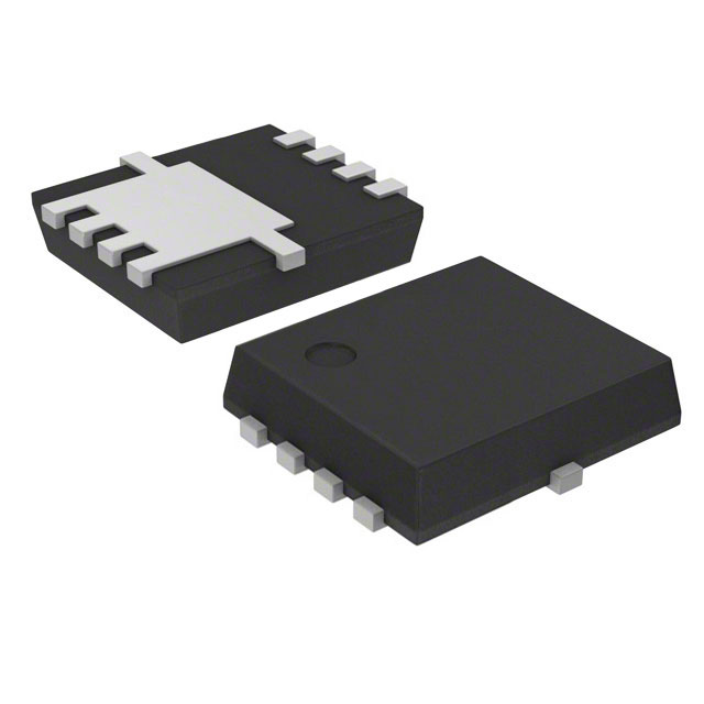
Texas Instruments_CSD19537Q3

Texas Instruments
CSD19537Q3  
Single FETs, MOSFETs

Texas Instruments
CSD19537Q3
278-CSD19537Q3
Ersa
Texas Instruments-CSD19537Q3-datasheets-1529851.pdf
MOSFET N-CH 100V 9.7A/50A 8VSON
In Stock : 2670

Not available to buy online? Want the lower wholesale price? Please Send RFQ to get best price, we will respond immediately

QUICK RFQ
ADD TO RFQ LIST
ersa FreeSample ersa flow
  • Quantity
  • Unit Price
  • Ext. Price
    • 1+
    • $1.04825
    • $1.05
    • 10+
    • $0.87271
    • $8.73
    • 30+
    • $0.78494
    • $23.55
    • 100+
    • $0.69718
    • $69.72
    ADD TO CART
    QUICK ORDER
    $1.04825    $1.05
    ISO9001
    Quality Policy
    ISO45001
    ISO14001

    CSD19537Q3 Description

    The CSD19537Q3 is a highly-integrated, single-chip motor controller from Texas Instruments (TI) designed for brushless DC (BLDC) motor control applications. It is part of TI's portfolio of motor control solutions that cater to a wide range of industrial, automotive, and consumer applications.

    Description:

    The CSD19537Q3 is a highly efficient and compact motor controller that combines a gate driver, power MOSFETs, and control logic into a single chip. It is specifically designed to control BLDC motors with a wide range of power levels and motor phases. The device is built on TI's proprietary CoolGaN™ technology, which enables high efficiency, low thermal dissipation, and high switching speeds.

    Features:

    1. Integrated gate driver and power MOSFETs: The CSD19537Q3 integrates the gate driver and power MOSFETs, reducing the need for external components and simplifying the overall system design.
    2. Wide input voltage range: The device can operate with a wide input voltage range, making it suitable for various power supply conditions.
    3. Advanced control algorithms: The CSD19537Q3 features advanced control algorithms, such as field-oriented control (FOC) and sensorless control, for improved motor performance and efficiency.
    4. High switching frequency: The device supports high switching frequencies, allowing for smaller and lighter motor control systems.
    5. Protection features: The CSD19537Q3 includes various protection features, such as overcurrent, overvoltage, and undervoltage protection, to ensure reliable operation and prevent damage to the motor and controller.
    6. Communication interfaces: The device offers communication interfaces, such as SPI or UART, for easy integration with microcontrollers and other system components.
    7. CoolGaN™ technology: The use of TI's CoolGaN™ technology enables high efficiency, low thermal dissipation, and high switching speeds.

    Applications:

    The CSD19537Q3 is suitable for a wide range of applications that require efficient and reliable BLDC motor control, including:

    1. Industrial applications: Servo drives, robotics, and automation systems.
    2. Automotive applications: Electric power steering (EPS), oil pumps, and cooling fans.
    3. Consumer applications: High-end appliances, power tools, and computer cooling systems.
    4. Renewable energy systems: Solar panel tracking systems and wind turbine control systems.
    5. Aerospace applications: Actuators and control systems for aircraft and drones.

    In summary, the CSD19537Q3 from Texas Instruments is a highly integrated, efficient, and versatile motor controller designed for BLDC motor control applications across various industries. Its advanced features, such as integrated gate drivers, power MOSFETs, and advanced control algorithms, make it an ideal choice for designers looking to create compact, efficient, and reliable motor control solutions.

    Tech Specifications

    Unit Weight
    Configuration
    Input Capacitance (Ciss) (Max) @ Vds
    Gate Charge (Qg) (Max) @ Vgs
    PPAP
    Fall Time
    Automotive
    RoHS
    Maximum IDSS (uA)
    Typical Turn-On Delay Time
    REACH Status
    Channel Type
    Rds(on) at VGS=10 V (max) (mΩ)
    Maximum Continuous Drain Current (A)
    VGSTH typ (typ) (V)
    Maximum Pulsed Drain Current @ TC=25°C (A)
    Operating temperature range (°C)
    Maximum Drain Source Voltage (V)
    Rds On (Max) @ Id, Vgs
    Standard Package Name
    Typical Reverse Recovery Charge (nC)
    Mounting
    Rise Time
    Current - Continuous Drain (Id) @ 25°C
    Typical Gate to Drain Charge (nC)
    Vgs th - Gate-Source Threshold Voltage
    Package
    Maximum Power Dissipation on PCB @ TC=25°C (W)
    Maximum Gate Resistance (Ohm)
    Logic level
    Typical Reverse Recovery Time (ns)
    Qg - Gate Charge
    Power Dissipation (Max)
    Process Technology
    Package Height
    Typical Gate to Source Charge (nC)
    Vgs (Max)
    Typical Drain Source Resistance @ 25°C (mOhm)
    Maximum Operating Temperature
    Width
    RoHS Status
    Typical Gate Threshold Voltage (V)
    SVHC Exceeds Threshold
    Transistor Polarity
    Typical Gate Charge @ 10V (nC)
    Maximum Diode Forward Voltage (V)
    Minimum Operating Temperature
    Vds - Drain-Source Breakdown Voltage
    Typical Diode Forward Voltage (V)
    Type
    Typical Output Capacitance (pF)
    Length
    Part Status
    Maximum Gate Threshold Voltage (V)
    Lead finish / Ball material
    Package Width
    Maximum Junction Ambient Thermal Resistance on PCB (°C/W)
    VGS (V)
    VDS (V)
    QGD (typ) (nC)
    Typical Turn-Off Delay Time (ns)
    Maximum Gate Source Leakage Current (nA)
    Id - Continuous Drain Current
    Typical Rise Time (ns)
    Channel Mode
    Typical Turn-On Delay Time (ns)
    Product Status
    Drain to Source Voltage (Vdss)
    Supplier Package
    Tradename
    ID - package limited (A)
    Transistor Type
    Package / Case
    Number of Channels
    Technology
    EU RoHS
    Carrier
    Rds On - Drain-Source Resistance
    ID - silicon limited at TC=25°C (A)
    Moisture Sensitivity Level (MSL)
    Operating Temperature
    Maximum Drain Source Resistance (mOhm)
    ECCN
    MSL rating / Peak reflow
    Mounting Type
    Vgs(th) (Max) @ Id
    Maximum Continuous Drain Current on PCB @ TC=25°C (A)
    Pin Count
    Minimum Gate Threshold Voltage (V)
    Typical Reverse Transfer Capacitance @ Vds (pF)
    Lead Shape
    SVHC
    Drive Voltage (Max Rds On, Min Rds On)
    HTSUS
    Pins
    USHTS
    Typical Gate Charge @ Vgs (nC)
    Typical Input Capacitance @ Vds (pF)
    Category
    PCB changed
    HTS
    FET Type
    Number of Elements per Chip
    Rating
    ECCN (US)
    Maximum Power Dissipation (mW)
    Supplier Device Package
    Minimum Operating Temperature (°C)
    Maximum Operating Temperature (°C)
    QG (typ) (nC)
    Typical Fall Time (ns)
    Maximum Positive Gate Source Voltage (V)
    Mfr
    Height
    Mounting Style
    FET Feature
    Maximum Gate Source Voltage (V)
    Vgs - Gate-Source Voltage
    Typical Gate Plateau Voltage (V)
    Typical Turn-Off Delay Time
    Material
    Package Length
    QGS (typ) (nC)
    REACH
    Series
    Operating Junction Temperature (°C)
    Pd - Power Dissipation
    Base Product Number

    CSD19537Q3 Documents

    Download datasheets and manufacturer documentation for CSD19537Q3

    Ersa CSD19537Q3 Symbol & Footprint by SnapMagic      
    Ersa CSD19537Q3 Unencrypted PSpice Model Package (Rev. B)       CSD19537Q3 TINA-TI Spice Model       CSD19537Q3 PSpice Model (Rev. A)      

    Shopping Guide

    Payment Methods
    Payment Methods include Prepayment TT (bank transfer), Western Union, and PayPal. Customers are responsible for shipping costs, bank charges, customs duties and taxes.
    Shipping Rate
    Shipments are made once a day around 5pm, excluding Sundays. Once shipped, the estimated delivery time is usually 5-7 business days, depending on the courier you choose.
    Delivery Methods
    Provide DHL, FedEx, UPS, EMS, SF Express and Registered Airmail International Delivery Service