
 German
 Japanese
 Portuguese
 Korea
Korea
 Mexico
 Dutch
Dutch


Texas Instruments
CSD18533KCS

Why Choose Us?
Professional Platform
B2B & B2C purchasingDelivery at full speed
1-2 days deliveryWide variety
Original manufacturers365 days guarantee
Responsible quality
.png)


Tech Specifications
CSD18533KCS Description
CSD18533KCS Description
The CSD18533KCS is a high-performance N-Channel MOSFET from Texas Instruments, designed for a wide range of applications requiring high power and efficiency. With a drain-to-source voltage (Vdss) of 60V and continuous drain current ratings of 72A at 25°C and 100A at case temperature, this MOSFET delivers exceptional performance in demanding power electronic applications.
CSD18533KCS Features
- High Power Handling: Capable of handling up to 100A of continuous drain current at case temperature, making it ideal for high-power applications.
- Low On-Resistance: With a maximum Rds(on) of 6.3mΩ at 75A and 10V Vgs, the CSD18533KCS offers low conduction losses, improving efficiency in power conversion systems.
- Robust Gate Drive: A maximum gate-source voltage (Vgs) of ±20V ensures reliable operation across a wide range of gate drive conditions.
- Low Gate Charge: A maximum gate charge (Qg) of 34nC at 10V Vgs contributes to fast switching speeds and reduced switching losses.
- High Input Capacitance: A maximum input capacitance (Ciss) of 3025pF at 30V Vds allows for high-frequency operation with minimal Miller effect.
- Thermal Management: Capable of dissipating up to 192W of power, making it suitable for applications with high thermal demands.
- Compliance and Standards: ROHS3 compliant and REACH unaffected, ensuring environmental and regulatory compliance.
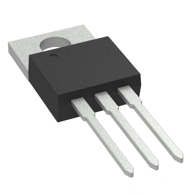
- Package Type: Available in a through-hole TO220-3 package, providing a robust and reliable mechanical solution for high-power applications.
CSD18533KCS Applications
The CSD18533KCS is well-suited for a variety of high-power applications, including:
- Power Supplies: Ideal for high-efficiency power conversion in switch-mode power supplies (SMPS) and uninterruptible power supplies (UPS).
- Motor Control: Effective in variable frequency drives (VFD) and electric vehicle (EV) motor control systems due to its high current and voltage ratings.
- Renewable Energy: Suitable for solar inverters and wind power converters, where high power and efficiency are critical.
- Industrial Automation: Reliable in high-power motor drives and industrial control systems that require robust and efficient power switching.
Conclusion of CSD18533KCS
The CSD18533KCS from Texas Instruments stands out for its high power handling, low on-resistance, and robust gate drive capabilities. Its compliance with environmental and regulatory standards, combined with its high thermal dissipation, makes it an excellent choice for a wide range of high-power applications. With its NexFET™ series pedigree, the CSD18533KCS offers a reliable and efficient solution for demanding power electronic systems.
FAQ
Not available to buy online? Want the lower wholesale price? Please Send RFQ to get best price, we will respond immediately


.png?x-oss-process=image/format,webp/resize,h_32)


