
 German
 Japanese
 Portuguese
 Korea
Korea
 Mexico
 Dutch
Dutch


Texas Instruments
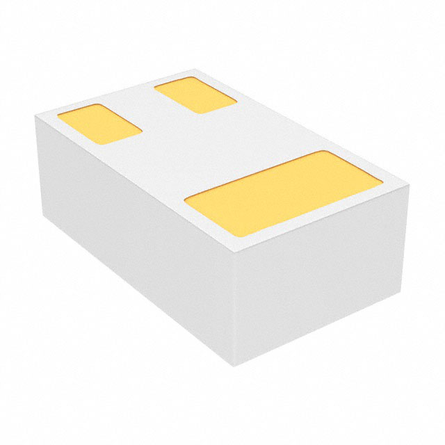
CSD25483F4

Why Choose Us?
Professional Platform
B2B & B2C purchasingDelivery at full speed
1-2 days deliveryWide variety
Original manufacturers365 days guarantee
Responsible quality
.png)


Tech Specifications
CSD25483F4 Description
The CSD25483F4 is a high performance, 4-channel Smart Gate Driver from Texas Instruments. It is designed to drive high voltage, high current MOSFETs in a variety of applications including electric vehicles, industrial motor drives, and renewable energy systems.
Description:
The CSD25483F4 is a monolithic, high voltage half-bridge gate driver with four independent channels. It is designed to drive N-channel MOSFETs in a wide range of applications. The device features a high voltage tolerant gate drive output, advanced desaturation detection, and spread spectrum clocking to reduce EMI.
Features:
- 4 independent gate driver channels
- High voltage tolerant gate drive output
- Advanced desaturation detection
- Spread spectrum clocking to reduce EMI
- Wide operating voltage range (10V to 60V)
- Low quiescent current
- Small package size (5mm x 7mm)
Applications:
- Electric vehicles (EVs)
- Industrial motor drives
- Renewable energy systems
- High voltage motor controllers
- Power supplies
- Servo drives
The CSD25483F4 is a versatile and high performance gate driver that can be used in a wide range of applications requiring high voltage and high current MOSFET driving capabilities. Its advanced features and small package size make it an ideal choice for space constrained applications.
FAQ
| Quantity | Unit Price | Ext. Price |
|---|---|---|
| 5+ | $0.16220 | $0.81 |
| 50+ | $0.12943 | $6.47 |
| 150+ | $0.11305 | $16.96 |
Not available to buy online? Want the lower wholesale price? Please Send RFQ to get best price, we will respond immediately


.png?x-oss-process=image/format,webp/resize,h_32)


