
 German
 Japanese
 Portuguese
 Korea
Korea
 Mexico
 Dutch
Dutch


Texas Instruments
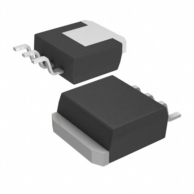
CSD18535KTT

Why Choose Us?
Professional Platform
B2B & B2C purchasingDelivery at full speed
1-2 days deliveryWide variety
Original manufacturers365 days guarantee
Responsible quality
.png)


Tech Specifications
CSD18535KTT Description
The CSD18535KTT is a high-performance, monolithic, synchronous, step-down (buck) regulator from Texas Instruments. It is designed to provide efficient and stable power conversion for a wide range of applications.
Description:
The CSD18535KTT is a highly integrated, high-efficiency, synchronous buck regulator that can operate from an input voltage range of 4.5V to 22V. It is available in a compact, thermally enhanced, 3mm x 3mm PowerTOP™-QFN package. The device features a wide output voltage range of 0.9V to 5.5V and can deliver up to 3A of continuous output current.
Features:
- High Efficiency: The CSD18535KTT offers high efficiency of up to 95%, which helps reduce power dissipation and improve overall system performance.
- Wide Input Voltage Range: The device can operate from an input voltage range of 4.5V to 22V, making it suitable for a variety of power supply sources.
- Wide Output Voltage Range: The output voltage can be programmed from 0.9V to 5.5V, providing flexibility for different load requirements.
- High Output Current: The device can deliver up to 3A of continuous output current, making it suitable for powering demanding loads.
- Synchronous Rectification: The CSD18535KTT uses synchronous rectification, which helps improve efficiency and reduce switching losses.
- Thermal Protection: The device features over-temperature protection and thermal shutdown to ensure safe operation and prevent damage due to overheating.
- Small Package Size: The 3mm x 3mm PowerTOP™-QFN package allows for easy integration into compact designs.
Applications:
The CSD18535KTT is suitable for a wide range of applications that require efficient and stable power conversion, including:
- Portable Electronics: Smartphones, tablets, and other mobile devices.
- Industrial Control Systems: Motor drives, sensor interfaces, and control panels.
- Medical Devices: Patient monitoring equipment, portable medical instruments, and wearable devices.
- Consumer Electronics: Smart home devices, gaming consoles, and portable audio players.
- Automotive Applications: Infotainment systems, lighting control, and sensor interfaces.
In summary, the CSD18535KTT from Texas Instruments is a high-efficiency, synchronous buck regulator that offers a wide input voltage range, high output current capability, and a compact package size. It is suitable for a variety of applications, including portable electronics, industrial control systems, medical devices, consumer electronics, and automotive applications.
FAQ
| Quantity | Unit Price | Ext. Price |
|---|---|---|
| 1+ | $2.66915 | $2.67 |
| 10+ | $2.61257 | $26.13 |
| 30+ | $2.57485 | $77.25 |
Not available to buy online? Want the lower wholesale price? Please Send RFQ to get best price, we will respond immediately


.png?x-oss-process=image/format,webp/resize,h_32)


