
 German
 Japanese
 Portuguese
 Korea
Korea
 Mexico
 Dutch
Dutch


STMicroelectronics
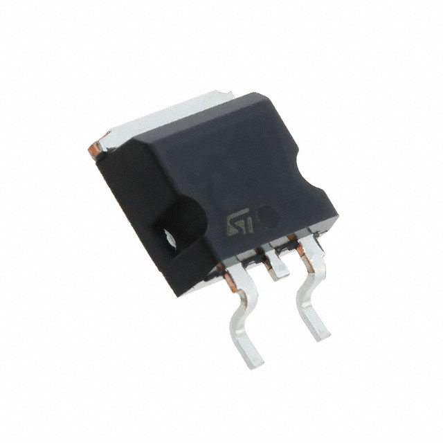
STB18NF30

Why Choose Us?
Professional Platform
B2B & B2C purchasingDelivery at full speed
1-2 days deliveryWide variety
Original manufacturers365 days guarantee
Responsible quality
.png)


Tech Specifications
STB18NF30 Description
STB18NF30 Description
The STB18NF30 is a high-performance N-channel MOSFET from STMicroelectronics, designed for automotive applications. With a drain-to-source voltage (Vdss) of 330V and a continuous drain current (Id) of 18A at 25°C, this device offers excellent electrical characteristics for demanding power management tasks. The STB18NF30 features a low on-resistance (Rds On) of 180mOhm at 9A and 10V, ensuring high efficiency in power conversion applications. Its high gate voltage (Vgs) of ±20V provides robust operation in various electronic systems.
STB18NF30 Features
- Low On-Resistance: The STB18NF30 boasts a maximum on-resistance (Rds On) of 180mOhm at 9A and 10V, which helps minimize power losses and improve efficiency in power conversion applications.
- High Drain-to-Source Voltage: With a Vdss of 330V, this MOSFET can handle high voltage applications, making it suitable for automotive and industrial power electronics.
- Robust Gate Voltage: The ±20V gate voltage rating ensures reliable operation in various electronic systems, providing flexibility in circuit design.
- Automotive Grade: Designed and qualified for automotive applications, the STB18NF30 offers robust performance in harsh environments.
- Surface Mount Package: The D2PAK package allows for easy integration into surface-mount printed circuit boards, enabling compact and efficient designs.
STB18NF30 Applications
The STB18NF30 is ideal for a variety of applications where high voltage and current handling are required, including:
- Automotive Power Management: Due to its automotive-grade qualification, the STB18NF30 is well-suited for power management in vehicles, such as battery management systems and electric power steering.
- Industrial Power Supplies: The high voltage and current ratings make this MOSFET suitable for power conversion in industrial applications, such as motor drives and power inverters.
- Renewable Energy Systems: The STB18NF30 can be used in solar power inverters and wind energy conversion systems, where high voltage and current handling are critical.
Conclusion of STB18NF30
The STB18NF30 from STMicroelectronics is a powerful N-channel MOSFET designed for high-voltage and high-current applications. Its low on-resistance, high drain-to-source voltage, and robust gate voltage make it an excellent choice for automotive and industrial power electronics. With its automotive-grade qualification and surface-mount package, the STB18NF30 offers a reliable and efficient solution for demanding power management tasks.
FAQ
| Quantity | Unit Price | Ext. Price |
|---|---|---|
| 10+ | $1.51663 | $15.17 |
| 30+ | $1.27543 | $38.26 |
| 100+ | $1.20275 | $120.28 |
| 500+ | $1.16983 | $584.91 |
| 1000+ | $1.15475 | $1154.75 |
Not available to buy online? Want the lower wholesale price? Please Send RFQ to get best price, we will respond immediately


.png?x-oss-process=image/format,webp/resize,h_32)


