

STMicroelectronics
STB75NF20
Single FETs, MOSFETs

Not available to buy online? Want the lower wholesale price? Please Send RFQ to get best price, we will respond immediately


.png?x-oss-process=image/format,webp/resize,p_30)


STB75NF20 Description
STB75NF20 Description
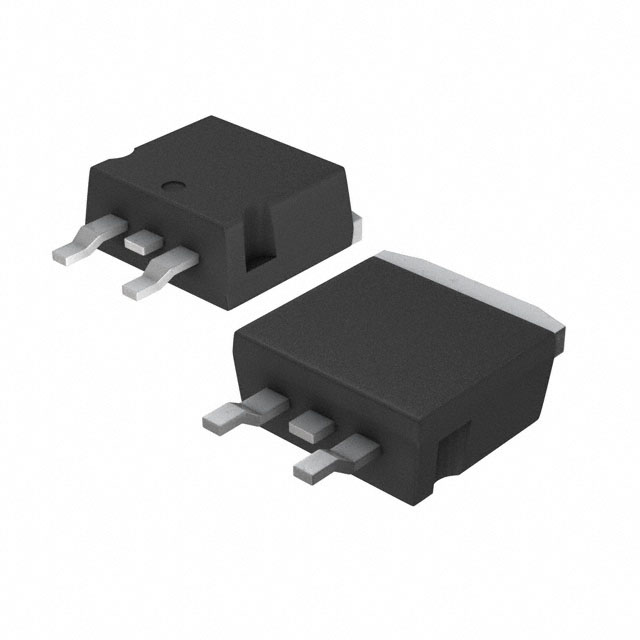
The STB75NF20 is a high-performance N-Channel MOSFET from STMicroelectronics, designed for applications requiring high current and voltage handling capabilities. With a drain-to-source voltage (Vdss) of 200V and a continuous drain current (Id) of 75A at 25°C, this device is well-suited for demanding power electronic applications. The STB75NF20 features a low on-resistance (Rds On) of 34mOhm at 37A and 10V, ensuring high efficiency and minimal power loss. The device is available in a D2PAK package, making it ideal for surface mount applications.
STB75NF20 Features
- 200V drain-to-source voltage (Vdss) for high voltage applications
- 75A continuous drain current (Id) at 25°C for high current handling
- Low on-resistance (Rds On) of 34mOhm at 37A and 10V for high efficiency
- D2PAK package for surface mount applications
- ±20V maximum gate-to-source voltage (Vgs) for robust operation
- 4V maximum threshold voltage (Vgs(th)) at 250µA for reliable switching
- 84nC maximum gate charge (Qg) at 10V for fast switching and low power consumption
- 3260pF maximum input capacitance (Ciss) at 25V for high-speed operation
- 190W maximum power dissipation (Tc) for high power applications
- REACH unaffected and RoHS3 compliant for environmental compliance
- Moisture sensitivity level (MSL) 1 for unlimited storage and handling
STB75NF20 Applications
The STB75NF20 is ideal for a wide range of high-power electronic applications, including:
- Power supplies and power conversion systems
- Motor drives and control systems
- Renewable energy systems, such as solar inverters and wind turbines
- Electric vehicle (EV) charging systems and power electronics
- Industrial automation and control systems
- High-power lighting systems, such as LED drivers and ballasts
Conclusion of STB75NF20
The STB75NF20 is a high-performance N-Channel MOSFET from STMicroelectronics, offering a combination of high voltage and current handling capabilities, low on-resistance, and fast switching speeds. Its robust design, compliance with environmental regulations, and wide range of applications make it an excellent choice for demanding power electronic systems. With its unique features and advantages over similar models, the STB75NF20 is a reliable and efficient solution for high-power applications in various industries.
Tech Specifications
STB75NF20 Documents
Download datasheets and manufacturer documentation for STB75NF20
Product Change Notification 2024-03-05 (PDF) D2PAK Leads (Pins) Modification (PDF) Product Change Notification (PDF) Related Parts


Shopping Guide


.png?x-oss-process=image/format,webp/resize,h_32)


©2025 ERSA Electronics Corporation.