STMicroelectronics_STF33N65M2

STMicroelectronics
STF33N65M2  
Single FETs, MOSFETs

STMicroelectronics
STF33N65M2
278-STF33N65M2
Ersa
STMicroelectronics-STF33N65M2-datasheets-12479549.pdf
MOSFET N-CH 650V 24A TO220FP
In Stock : 990

Not available to buy online? Want the lower wholesale price? Please Send RFQ to get best price, we will respond immediately

QUICK RFQ
ADD TO RFQ LIST
ersa FreeSample ersa flow
ISO9001
Quality Policy
ISO45001
ISO14001

STF33N65M2 Description

STF33N65M2 Description

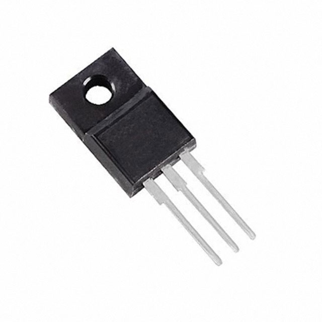
The STF33N65M2 is a high-performance N-Channel MOSFET from STMicroelectronics, designed for applications requiring high voltage and current handling capabilities. With a drain-to-source voltage (Vdss) of 650V and a continuous drain current (Id) of 24A at 25°C, this device is ideal for use in various power electronics applications. The STF33N65M2 features a low on-resistance (Rds On) of 140mOhm at 12A and 10V, ensuring efficient power dissipation and reduced power loss. The device is mounted in a through-hole TO220FP package, making it suitable for a wide range of applications.

STF33N65M2 Features

  • High drain-to-source voltage (Vdss) of 650V for reliable high-voltage operation
  • Continuous drain current (Id) of 24A at 25°C for efficient current handling
  • Low on-resistance (Rds On) of 140mOhm at 12A and 10V for reduced power loss
  • Through-hole TO220FP package for easy integration into various applications
  • Active product status, ensuring ongoing availability and support
  • REACH unaffected and RoHS3 compliant, meeting environmental and regulatory requirements
  • Moisture sensitivity level (MSL) of 1, allowing for unlimited storage time
  • Operating temperature range of -55°C to 150°C (TJ) for use in a variety of environments

STF33N65M2 Applications

The STF33N65M2 is ideal for use in a wide range of power electronics applications, including:

  1. Motor control and drives
  2. Power supplies and converters
  3. Automotive electronics
  4. Industrial control systems
  5. Renewable energy systems, such as solar inverters and wind turbines
  6. High-voltage switching and protection circuits

Conclusion of STF33N65M2

The STF33N65M2 is a versatile and high-performance N-Channel MOSFET that offers excellent voltage and current handling capabilities, making it an ideal choice for a wide range of power electronics applications. Its low on-resistance, high-voltage rating, and compliance with environmental and regulatory standards make it a preferred choice over similar models. With its robust performance and reliable operation, the STF33N65M2 is a valuable addition to any power electronics design.

Tech Specifications

Unit Weight
Configuration
Input Capacitance (Ciss) (Max) @ Vds
Gate Charge (Qg) (Max) @ Vgs
PPAP
Fall Time
Automotive
RoHS
Maximum IDSS (uA)
Typical Turn-On Delay Time
REACH Status
Channel Type
Maximum Continuous Drain Current (A)
Maximum Pulsed Drain Current @ TC=25°C (A)
Maximum Drain Source Voltage (V)
Supplier Temperature Grade
Rds On (Max) @ Id, Vgs
Standard Package Name
Typical Reverse Recovery Charge (nC)
Mounting
Rise Time
Current - Continuous Drain (Id) @ 25°C
Typical Gate to Drain Charge (nC)
Vgs th - Gate-Source Threshold Voltage
Package
Typical Reverse Recovery Time (ns)
Qg - Gate Charge
Power Dissipation (Max)
Process Technology
Package Height
Typical Gate to Source Charge (nC)
Vgs (Max)
Maximum Operating Temperature
RoHS Status
Typical Gate Threshold Voltage (V)
SVHC Exceeds Threshold
Transistor Polarity
Typical Gate Charge @ 10V (nC)
Maximum Diode Forward Voltage (V)
Minimum Operating Temperature
Vds - Drain-Source Breakdown Voltage
Typical Output Capacitance (pF)
Tab
Part Status
Maximum Gate Threshold Voltage (V)
Package Width
Typical Turn-Off Delay Time (ns)
Maximum Gate Source Leakage Current (nA)
Id - Continuous Drain Current
Typical Rise Time (ns)
Channel Mode
Typical Turn-On Delay Time (ns)
Product Status
Drain to Source Voltage (Vdss)
Supplier Package
Tradename
Transistor Type
Package / Case
Number of Channels
Technology
EU RoHS
Rds On - Drain-Source Resistance
Moisture Sensitivity Level (MSL)
Operating Temperature
Maximum Drain Source Resistance (mOhm)
ECCN
Mounting Type
Vgs(th) (Max) @ Id
Pin Count
Minimum Gate Threshold Voltage (V)
Typical Reverse Transfer Capacitance @ Vds (pF)
Lead Shape
SVHC
Drive Voltage (Max Rds On, Min Rds On)
HTSUS
USHTS
Typical Gate Charge @ Vgs (nC)
Typical Input Capacitance @ Vds (pF)
Category
PCB changed
HTS
FET Type
Number of Elements per Chip
ECCN (US)
Maximum Power Dissipation (mW)
Supplier Device Package
Minimum Operating Temperature (°C)
Maximum Operating Temperature (°C)
Typical Fall Time (ns)
Maximum Positive Gate Source Voltage (V)
Mfr
Mounting Style
FET Feature
Maximum Gate Source Voltage (V)
Vgs - Gate-Source Voltage
Typical Gate Plateau Voltage (V)
Typical Turn-Off Delay Time
Package Length
Series
Operating Junction Temperature (°C)
Pd - Power Dissipation
Base Product Number
Grade
ECCN (EU)
RoHs compliant

STF33N65M2 Documents

Download datasheets and manufacturer documentation for STF33N65M2

Ersa Mult Dev Wafer Site Add 3/Aug/2018      
Ersa STx33N65M2      
Ersa Box Label Chg 28/Jul/2016      
Ersa STx33N65M2      

Shopping Guide

Payment Methods
Payment Methods include Prepayment TT (bank transfer), Western Union, and PayPal. Customers are responsible for shipping costs, bank charges, customs duties and taxes.
Shipping Rate
Shipments are made once a day around 5pm, excluding Sundays. Once shipped, the estimated delivery time is usually 5-7 business days, depending on the courier you choose.
Delivery Methods
Provide DHL, FedEx, UPS, EMS, SF Express and Registered Airmail International Delivery Service