
STMicroelectronics
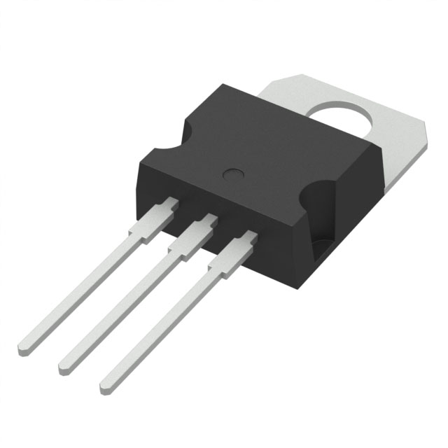
STP55NF06L
Single FETs, MOSFETs


- 1+
- $1.22875
- $1.23
- 10+
- $1.04494
- $10.45
- 50+
- $0.94392
- $47.2

.png?x-oss-process=image/format,webp/resize,p_30)


STP55NF06L Description
The STP55NF06L is a high-power, high-voltage N-channel MOSFET manufactured by STMicroelectronics. Here is a description of the model, its features, and applications:
Description:
The STP55NF06L is an N-channel enhancement mode field-effect transistor (FET) that is designed for high-power applications. It is a member of the STPOWER family of MOSFETs, which are optimized for use in automotive and industrial applications.
Features:
- High Power: The STP55NF06L is designed to handle high power levels, with a continuous drain current (Id) of up to 49A and a drain-source voltage (Vdss) of up to 60V.
- Low On-State Resistance: The device has a low on-state resistance (Rdson) of 55mΩ max, which helps to minimize power dissipation and improve efficiency in power conversion applications.
- Avalanche Energy Capable: The STP55NF06L is designed to withstand high energy pulses during avalanche transients, making it suitable for use in applications that may experience high-energy transients.
- Integrated Bootstrap Diode: The device features an integrated bootstrap diode, which helps to reduce switching losses and improve efficiency in power conversion applications.
- Robustness: The STP55NF06L is designed to be robust and reliable, with built-in protection features such as over-temperature protection and over-current protection.
Applications:
The STP55NF06L is suitable for a wide range of high-power applications, including:
- Motor Control: The device can be used in motor control applications such as electric vehicles, industrial automation, and robotics.
- Power Conversion: The STP55NF06L is well-suited for use in power conversion applications such as DC-DC converters, AC-DC converters, and solar inverters.
- Automotive Applications: The device is designed to meet the stringent requirements of automotive applications, making it suitable for use in electric and hybrid vehicles.
- Industrial Applications: The STP55NF06L can be used in various industrial applications such as power supplies, UPS systems, and motor drives.
Overall, the STP55NF06L is a high-power, high-voltage MOSFET that offers excellent performance and reliability for a wide range of applications. Its low on-state resistance, integrated bootstrap diode, and robustness make it an ideal choice for power conversion and motor control applications.
Tech Specifications
STP55NF06L Documents
Download datasheets and manufacturer documentation for STP55NF06L
 N-Channel STripFET 2nd Generation Products Capacity Extension in ST s Ang Mo Kio (Singapore) FAB (PDF) TO-220 ECOPACK 2 graded moulding compound assembly capacity expansion - Subcontractor PSI Laguna (Philippines) (PDF) Product / Process Change Notification (PDF) Product Change Notification (PDF) Product Change Notification 2024-04-04 (PDF) PRODUCT CHANGE NOTIFICATION (PDF)
  STP55NF06L Symbol & Footprint by SnapMagic
 Shopping Guide


.png?x-oss-process=image/format,webp/resize,h_32)


