
STMicroelectronics
STW26NM50
Single FETs, MOSFETs


.png?x-oss-process=image/format,webp/resize,p_30)


STW26NM50 Description
STW26NM50 Description
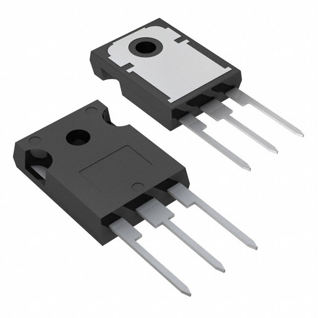
The STW26NM50 is a high-performance N-Channel MOSFET designed and manufactured by STMicroelectronics. This device is part of the MDmesh™ series and is offered in a TO247-3 package. With a drain-to-source voltage (Vdss) of 500V and a continuous drain current (Id) of 30A at 25°C, the STW26NM50 is suitable for various high-power applications. The device is designed to operate at an elevated junction temperature of 150°C (TJ) and has a maximum power dissipation of 313W (Tc). The STW26NM50 is compliant with the RoHS3 standard and is classified as REACH unaffected.
STW26NM50 Features
- High Voltage and Current Ratings: The STW26NM50 boasts a drain-to-source voltage (Vdss) of 500V and a continuous drain current (Id) of 30A at 25°C, making it suitable for high-power applications.
- Low On-Resistance: The device features a maximum on-resistance (Rds On) of 120mOhm at 13A and 10V, contributing to high efficiency in power management.
- Gate Charge and Input Capacitance: The STW26NM50 has a maximum gate charge (Qg) of 106 nC at 10V and an input capacitance (Ciss) of 3000 pF at 25V, ensuring fast switching and reduced power loss.
- Robust Operating Temperature: The device can operate at a junction temperature of up to 150°C (TJ), making it suitable for applications with high thermal demands.
- Compliance and Environmental Standards: The STW26NM50 is compliant with RoHS3 and is classified as REACH unaffected, ensuring environmental responsibility.
STW26NM50 Applications
The STW26NM50 is ideal for various high-power applications due to its high voltage and current ratings, low on-resistance, and robust operating temperature. Some specific use cases include:
- Power Supplies: The STW26NM50 can be used in power supply designs, such as switch-mode power supplies (SMPS) and uninterruptible power supplies (UPS), where high efficiency and reliability are critical.
- Industrial Control Systems: The device is suitable for motor control applications in industrial settings, where high power and temperature resistance are required.
- Automotive Applications: The STW26NM50 can be used in automotive systems, such as electric vehicle (EV) chargers and power management systems, where high voltage and current ratings are essential.
Conclusion of STW26NM50
The STW26NM50 is a high-performance N-Channel MOSFET from STMicroelectronics, offering a combination of high voltage and current ratings, low on-resistance, and robust operating temperature. Its compliance with RoHS3 and REACH unaffected status ensures environmental responsibility. The STW26NM50 is ideal for high-power applications, such as power supplies, industrial control systems, and automotive applications, where performance and reliability are paramount.
Tech Specifications
STW26NM50 Documents
Download datasheets and manufacturer documentation for STW26NM50
 IPG/14/8475 16/May/2014
  STW26NM50
  Standard outer labelling 15/Nov/2023
  STW26NM50 View All Specifications
  STW26NM50
 Shopping Guide


.png?x-oss-process=image/format,webp/resize,h_32)


