
STMicroelectronics
STB11NK50ZT4
Single FETs, MOSFETs


.png?x-oss-process=image/format,webp/resize,p_30)


STB11NK50ZT4 Description
STB11NK50ZT4 Description
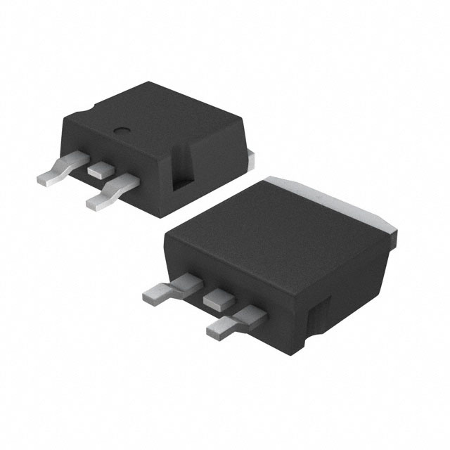
The STB11NK50ZT4 is a high-performance N-Channel MOSFET from STMicroelectronics, designed for applications requiring high voltage and current capabilities. It features a D2PAK package, making it suitable for surface mount applications. With a drain-source voltage (Vdss) of 500V and a continuous drain current (Id) of 10A at 25°C, this MOSFET is ideal for demanding power electronics applications.
STB11NK50ZT4 Features
- High Voltage and Current Ratings: The STB11NK50ZT4 boasts a drain-source voltage (Vdss) of 500V and a continuous drain current (Id) of 10A at 25°C, making it suitable for high-power applications.
- Low On-Resistance: With a maximum Rds(on) of 520mOhm at 4.5A and 10V, this MOSFET offers low power dissipation and high efficiency.
- Fast Switching Speed: The STB11NK50ZT4 has a low gate charge (Qg) of 68nC at 10V, enabling fast switching and reducing switching losses.
- Robust Package: The D2PAK package provides excellent thermal performance and mechanical robustness, making it suitable for high-power applications.
- Compliance with Regulations: The STB11NK50ZT4 is REACH unaffected, RoHS3 compliant, and EAR99 classified, ensuring compliance with environmental and trade regulations.
STB11NK50ZT4 Applications
The STB11NK50ZT4 is ideal for a variety of high-power applications, including:
- Power Supplies: Its high voltage and current ratings make it suitable for use in power supply designs, such as switching power supplies and battery chargers.
- Motor Control: The STB11NK50ZT4's low on-resistance and fast switching speed make it an excellent choice for motor control applications, including brushless DC motors and stepper motors.
- Industrial Automation: Its robust package and high power ratings make it suitable for use in industrial automation equipment, such as servo drives and robotic systems.
- Renewable Energy: The STB11NK50ZT4 can be used in renewable energy applications, such as solar inverters and wind power converters, due to its high voltage and current capabilities.
Conclusion of STB11NK50ZT4
The STB11NK50ZT4 is a high-performance N-Channel MOSFET from STMicroelectronics, offering a combination of high voltage, current, and power ratings, low on-resistance, and fast switching speed. Its robust D2PAK package and compliance with environmental and trade regulations make it an ideal choice for a wide range of high-power applications, including power supplies, motor control, industrial automation, and renewable energy systems.
Tech Specifications
STB11NK50ZT4 Documents
Download datasheets and manufacturer documentation for STB11NK50ZT4
 D2PAK Leads (Pins) Modification (PDF) Product / Process Change Notification (PDF)
 Shopping Guide


.png?x-oss-process=image/format,webp/resize,h_32)


