
STMicroelectronics
STW28NM50N
Single FETs, MOSFETs


.png?x-oss-process=image/format,webp/resize,p_30)


STW28NM50N Description
STW28NM50N Description
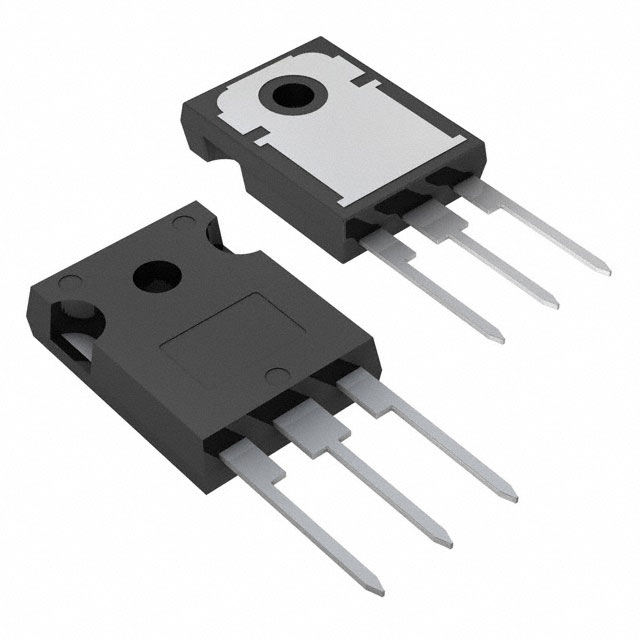
The STW28NM50N from STMicroelectronics is a high-performance N-channel MOSFET designed for demanding power applications. With a 500V drain-to-source voltage (Vdss) and 21A continuous drain current (Id), it delivers robust power handling in a TO-247-3 package. Built using MDmesh™ II technology, this MOSFET offers superior switching efficiency and thermal performance, making it ideal for high-voltage, high-frequency applications. Its low on-resistance (Rds(on) of 158mΩ @ 10V Vgs) ensures minimal conduction losses, while the ±25V gate-source voltage (Vgs) tolerance provides flexibility in drive circuitry. The device operates reliably up to 150°C junction temperature (TJ) and is RoHS3 compliant, meeting stringent environmental standards.
STW28NM50N Features
- High Voltage & Current Rating: 500V Vdss and 21A Id for robust power switching.
- Low Rds(on): 158mΩ @ 10V Vgs, reducing conduction losses and improving efficiency.
- Advanced MDmesh™ II Technology: Enhances switching speed and reduces parasitic effects.
- High Gate Charge (Qg): 50nC @ 10V, optimized for fast switching applications.
- Wide Vgs Range: ±25V, offering design flexibility.
- Thermal Performance: 150W power dissipation (Tc) and 150°C TJ for reliable operation in harsh environments.
- Compliance: ROHS3, REACH unaffected, and ECCN EAR99 for global usability.
STW28NM50N Applications
The STW28NM50N excels in high-efficiency power systems, including:
- Switched-Mode Power Supplies (SMPS): High-voltage DC-DC converters and PFC stages.
- Motor Drives & Inverters: Industrial and automotive motor control systems.
- Renewable Energy Systems: Solar inverters and wind power converters.
- Inductive Load Switching: Relays, solenoids, and high-current switching circuits.
- Audio Amplifiers: Class-D amplifier output stages for high-fidelity audio.
Conclusion of STW28NM50N
The STW28NM50N stands out as a high-reliability MOSFET for 500V power applications, combining low Rds(on), fast switching, and excellent thermal performance. Its MDmesh™ II technology ensures efficiency in demanding environments, while its TO-247-3 package provides mechanical robustness. Whether in industrial power systems, renewable energy, or motor control, this MOSFET delivers superior performance and durability, making it a top choice for engineers prioritizing efficiency and reliability.
Tech Specifications
STW28NM50N Documents
Download datasheets and manufacturer documentation for STW28NM50N
 IPG-PWR/14/8674 02/Sep/2014
  STx28NM50N
  Standard outer labelling 15/Nov/2023
  STW28NM50N View All Specifications
  STx28NM50N
 Shopping Guide


.png?x-oss-process=image/format,webp/resize,h_32)


