
STMicroelectronics
STW43N60DM2
Single FETs, MOSFETs


.png?x-oss-process=image/format,webp/resize,p_30)


STW43N60DM2 Description
STW43N60DM2 Description
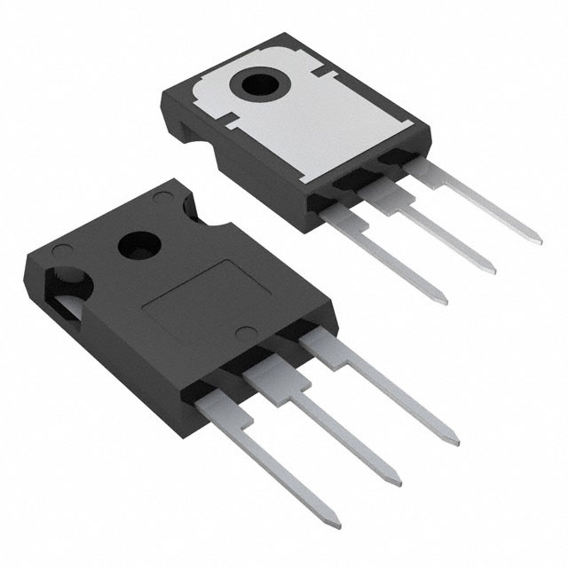
The STW43N60DM2 is a high-performance MOSFET N-CH 600V 34A TO247 from STMicroelectronics, designed for demanding applications that require high power dissipation and efficient switching. This device leverages advanced MOSFET technology to deliver superior performance and reliability.
STW43N60DM2 Features
- Input Capacitance (Ciss): The STW43N60DM2 boasts an ultra-low input capacitance of 2500 pF @ 100 V, enabling fast switching speeds and reduced power consumption.
- Gate Charge (Qg): With a maximum gate charge of 56 nC @ 10 V, this MOSFET offers efficient gate control and reduced gate driver requirements.
- Drain to Source Voltage (Vdss): Capable of handling voltages up to 600 V, the STW43N60DM2 is suitable for high-voltage applications.
- Power Dissipation: The device can dissipate up to 250W (Tc), making it ideal for power electronics.
- Rds On (Max): The STW43N60DM2 achieves a low on-resistance of 93mOhm @ 17A, 10V, which minimizes power losses and improves efficiency.
- Vgs(th) (Max): A threshold voltage of 5V @ 250µA ensures reliable operation and consistent performance.
- Series: The MDmesh™ DM2 series offers advanced features and performance benefits over standard models.
- Current - Continuous Drain (Id): The device can handle continuous drain currents of up to 34A (Tc) at 25°C, making it suitable for high-current applications.
STW43N60DM2 Applications
The STW43N60DM2 is ideal for a variety of applications where high power, efficiency, and reliability are critical:
- Power Electronics: Due to its high power dissipation and low on-resistance, the STW43N60DM2 is well-suited for power electronics applications such as power supplies, converters, and inverters.
- Industrial Automation: The device's high voltage and current ratings make it an excellent choice for motor drives and control systems in industrial automation.
- Automotive: The STW43N60DM2 can be used in automotive applications such as electric vehicle charging systems, powertrain control, and battery management systems.
Conclusion of STW43N60DM2
The STW43N60DM2 from STMicroelectronics is a powerful MOSFET designed for high-performance applications. Its unique combination of low input capacitance, low on-resistance, and high voltage and current ratings make it an excellent choice for power electronics, industrial automation, and automotive applications. With its advanced features and performance benefits, the STW43N60DM2 offers a reliable and efficient solution for demanding electronic systems.
Tech Specifications
STW43N60DM2 Documents
Download datasheets and manufacturer documentation for STW43N60DM2
 Wafer 15/Feb/2019
  STW43N60DM2
  Standard outer labelling 15/Nov/2023
  STW43N60DM2
 Shopping Guide


.png?x-oss-process=image/format,webp/resize,h_32)


