
STMicroelectronics
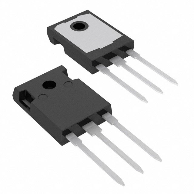
STWA72N60DM2AG
Single FETs, MOSFETs


.png?x-oss-process=image/format,webp/resize,p_30)


STWA72N60DM2AG Description
STWA72N60DM2AG Description
The STWA72N60DM2AG is a high-performance N-Channel MOSFET from STMicroelectronics, designed for use in a variety of applications requiring high voltage and current handling capabilities. With a drain-to-source voltage of 600V and a continuous drain current of 66A at 25°C, this MOSFET is well-suited for demanding automotive and industrial applications.
STWA72N60DM2AG Features
- 600V Drain-to-Source Voltage (Vdss): Capable of handling high voltage applications, making it ideal for use in automotive and industrial electronics.
- 66A Continuous Drain Current (Id) @ 25°C: Provides ample current handling capabilities for demanding applications.
- 42mOhm Rds On (Max) @ 33A, 10V: Offers low on-resistance for efficient power dissipation.
- 5508 pF Input Capacitance (Ciss) (Max) @ 100V: Minimizes input capacitance, reducing power loss and improving performance.
- 121 nC Gate Charge (Qg) (Max) @ 10V: Reduces switching losses and improves efficiency.
- 5V Vgs(th) (Max) @ 250µA: Provides a low threshold voltage for easier gate drive.
- ±25V Vgs (Max): Allows for a wide range of gate voltages, increasing flexibility in circuit design.
- 446W Power Dissipation (Max): Capable of dissipating high amounts of power, making it suitable for high-power applications.
- ROHS3 Compliant: Ensures environmental compliance and meets industry standards.
- REACH Unaffected: Complies with the European Union's Registration, Evaluation, Authorization, and Restriction of Chemicals (REACH) regulations.
- Moisture Sensitivity Level (MSL) 1: Indicates that the device is not sensitive to moisture, allowing for easier handling and storage.
- Automotive Grade: Designed to meet the stringent requirements of the automotive industry.
STWA72N60DM2AG Applications
The STWA72N60DM2AG is ideal for use in a variety of applications, including:
- Automotive Electronics: Due to its high voltage and current handling capabilities, as well as its automotive grade rating, this MOSFET is well-suited for use in automotive electronics, such as electric vehicle charging systems, powertrain control modules, and battery management systems.
- Industrial Electronics: Its high power dissipation and robust performance make it suitable for use in industrial electronics, such as motor drives, power supplies, and renewable energy systems.
- Power Management: The STWA72N60DM2AG's low on-resistance and high current handling capabilities make it ideal for use in power management applications, such as power factor correction circuits and DC-DC converters.
Conclusion of STWA72N60DM2AG
The STWA72N60DM2AG is a high-performance N-Channel MOSFET from STMicroelectronics that offers a combination of high voltage and current handling capabilities, low on-resistance, and low gate charge. Its automotive grade rating, ROHS3 compliance, and REACH unaffected status make it an ideal choice for use in demanding automotive and industrial applications. With its unique features and advantages over similar models, the STWA72N60DM2AG is a reliable and efficient solution for a wide range of high-power applications.
Tech Specifications
STWA72N60DM2AG Documents
Download datasheets and manufacturer documentation for STWA72N60DM2AG
 STWA72N60DM2AG
 Shopping Guide


.png?x-oss-process=image/format,webp/resize,h_32)


