
Texas Instruments
CSD18543Q3AT
Single FETs, MOSFETs


.png?x-oss-process=image/format,webp/resize,p_30)


CSD18543Q3AT Description
CSD18543Q3AT Description
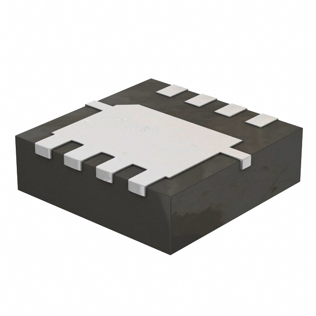
The CSD18543Q3AT is a high-performance MOSFET (Metal Oxide) from Texas Instruments, designed for applications that require efficient power management and high current handling capabilities. This N-Channel MOSFET features a drain-to-source voltage (Vdss) of 60V, a continuous drain current (Id) of 12A at 25°C and 60A at case temperature (Tc), and a maximum power dissipation of 66W. With its NexFET™ series, this device offers superior performance and reliability.
CSD18543Q3AT Features
- Technology: MOSFET (Metal Oxide)
- Drain to Source Voltage (Vdss): 60V
- Current - Continuous Drain (Id): 12A (Ta), 60A (Tc)
- Power Dissipation (Max): 66W (Tc)
- Rds On (Max) @ Id, Vgs: 15.6mOhm @ 12A, 4.5V
- Vgs(th) (Max) @ Id: 2.7V @ 250µA
- Input Capacitance (Ciss) (Max) @ Vds: 1150 pF @ 30 V
- Gate Charge (Qg) (Max) @ Vgs: 14.5 nC @ 10 V
- Drive Voltage (Max Rds On, Min Rds On): 4.5V, 10V
- Vgs (Max): ±20V
- Mounting Type: Surface Mount
- Moisture Sensitivity Level (MSL): 1 (Unlimited)
- REACH Status: REACH Unaffected
- RoHS Status: ROHS3 Compliant
- ECCN: EAR99
- Package: Tape & Reel (TR)
CSD18543Q3AT Applications
The CSD18543Q3AT is ideal for a variety of applications where high efficiency and power handling are critical. Some specific use cases include:
- Power Management: In power supply designs, this MOSFET can handle high currents with low on-resistance, reducing power losses and improving efficiency.
- Motor Control: Its high current capability and low gate charge make it suitable for motor control applications, where fast switching and high efficiency are required.
- Automotive Applications: The device's robustness and high power dissipation capability make it suitable for automotive applications, such as electric vehicle chargers and powertrain control systems.
- Industrial Control: In industrial control systems, the CSD18543Q3AT can be used for high-power switching and motor control, providing reliable performance in demanding environments.
Conclusion of CSD18543Q3AT
The CSD18543Q3AT from Texas Instruments is a powerful MOSFET designed for high-efficiency power management and motor control applications. Its NexFET™ technology, combined with its high drain current and low on-resistance, make it an excellent choice for demanding applications. With its REACH unaffected status, RoHS3 compliance, and moisture sensitivity level 1, this device is not only high-performing but also environmentally friendly and reliable. The CSD18543Q3AT is a versatile and powerful solution for engineers looking to optimize power efficiency and performance in their designs.
Tech Specifications
CSD18543Q3AT Documents
Download datasheets and manufacturer documentation for CSD18543Q3AT
 CSD18543Q3A
  CSD18543Q3A
 Shopping Guide


.png?x-oss-process=image/format,webp/resize,h_32)


