
STMicroelectronics
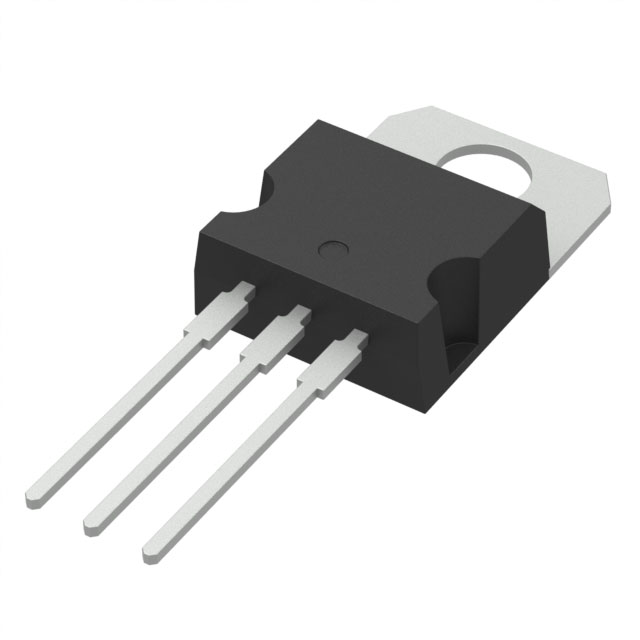
STP80NF70
Single FETs, MOSFETs


- 1+
- $0.96214
- $0.96
- 10+
- $0.79985
- $8
- 30+
- $0.71870
- $21.56
- 100+
- $0.63756
- $63.76
- 500+
- $0.58954
- $294.77
- 1000+
- $0.56470
- $564.7

.png?x-oss-process=image/format,webp/resize,p_30)


STP80NF70 Description
STP80NF70 Description
The STP80NF70 is a high-performance N-Channel MOSFET from STMicroelectronics, designed for demanding applications that require high voltage and current handling capabilities. With a drain-to-source voltage (Vdss) of 68V and a continuous drain current (Id) of 98A at 25°C, this device is well-suited for power electronics and motor control applications. The STP80NF70 is built using advanced MOSFET technology, ensuring high efficiency and reliability in operation.
STP80NF70 Features
- High Voltage and Current Handling: The STP80NF70 can handle a maximum drain-to-source voltage of 68V and a continuous drain current of 98A at 25°C, making it ideal for high-power applications.
- Low On-Resistance: The device features a maximum on-resistance (Rds On) of 9.8mOhm at 40A and 10V, contributing to high efficiency and low power loss in the circuit.
- Robust Gate Drive: With a maximum gate-source voltage (Vgs) of ±20V and a threshold voltage (Vgs(th)) of 4V at 250µA, the STP80NF70 provides robust gate drive capabilities for reliable operation.
- Low Input Capacitance: The device has a maximum input capacitance (Ciss) of 2550 pF at 25V, which helps reduce switching losses and improve overall performance.
- Gate Charge Optimization: The maximum gate charge (Qg) is 75 nC at 10V, enabling fast switching and minimizing power dissipation.
- Thermal Management: The STP80NF70 can dissipate up to 190W of power (Tc), ensuring stable operation in high-temperature environments.
- Environmental Compliance: The device is compliant with the RoHS3 directive and has a moisture sensitivity level (MSL) of 1, indicating unlimited storage time before reflow soldering.
STP80NF70 Applications
The STP80NF70 is an excellent choice for a variety of high-power applications, including:
- Power Electronics: Due to its high voltage and current ratings, the STP80NF70 is ideal for power conversion and regulation in various electronic systems.
- Motor Control: The device's low on-resistance and fast switching capabilities make it suitable for motor drive applications, such as electric vehicles and industrial automation.
- Industrial Automation: The STP80NF70 can be used in high-power industrial control systems, where reliability and efficiency are critical.
- Renewable Energy Systems: The device's high voltage and current ratings make it suitable for use in solar inverters and wind power systems.
Conclusion of STP80NF70
The STP80NF70 from STMicroelectronics is a high-performance N-Channel MOSFET designed for demanding high-power applications. Its combination of high voltage and current ratings, low on-resistance, and robust gate drive capabilities make it an ideal choice for power electronics, motor control, and industrial automation systems. While it is not recommended for new designs, the STP80NF70 remains a reliable and efficient solution for existing applications that require its specific performance characteristics.
Tech Specifications
STP80NF70 Documents
Download datasheets and manufacturer documentation for STP80NF70
 STP80NF70
  STP80NF70 View All Specifications
  STP80NF70
 Shopping Guide


.png?x-oss-process=image/format,webp/resize,h_32)


