

Texas Instruments
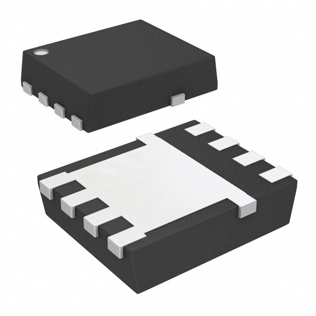
CSD17311Q5
Single FETs, MOSFETs

Not available to buy online? Want the lower wholesale price? Please Send RFQ to get best price, we will respond immediately


.png?x-oss-process=image/format,webp/resize,p_30)


CSD17311Q5 Description
CSD17311Q5 Description
The CSD17311Q5 from Texas Instruments is a high-performance N-channel MOSFET designed for power management applications. Part of the NexFET™ series, it features a 30V drain-to-source voltage (Vdss) and delivers 32A continuous drain current (Id) at 25°C (Ta), or 100A when mounted on a heatsink (Tc). With an ultra-low on-resistance (Rds(on)) of just 2mΩ at 30A and 8V gate drive, this MOSFET minimizes conduction losses, improving efficiency in high-current applications. Its surface-mount 8VSON package ensures compact PCB integration, while Tape & Reel (TR) packaging facilitates automated assembly.
CSD17311Q5 Features
- Low Rds(on): 2mΩ @ 30A, 8V ensures minimal power dissipation.
- High Current Handling: Supports 32A (Ta) / 100A (Tc), ideal for demanding loads.
- Fast Switching: Low gate charge (Qg) of 31nC @ 4.5V and input capacitance (Ciss) of 4280pF @ 15V enhance switching efficiency.
- Robust Drive Voltage Range: Operates efficiently at 3V to 8V gate drive.
- Reliable & Compliant: ROHS3, REACH Unaffected, ECCN EAR99, and MSL 1 (Unlimited) for broad industrial use.
- Thermal Performance: 3.2W max power dissipation ensures stability under load.
CSD17311Q5 Applications
- DC-DC Converters & Voltage Regulators: Optimized for synchronous buck converters in computing and telecom.
- Motor Drives & H-Bridges: Low Rds(on) reduces heat in brushed/BLDC motor controllers.
- Battery Management Systems (BMS): Efficient power switching in Li-ion/PbA protection circuits.
- Load Switches & Hot-Swap Circuits: High current tolerance suits server/SSD power distribution.
- Automotive & Industrial Power Systems: Compact footprint and reliability for 12V/24V systems.
Conclusion of CSD17311Q5
The CSD17311Q5 stands out for its ultra-low Rds(on), high current capacity, and fast switching, making it a superior choice for power-efficient designs. Its NexFET™ technology and 8VSON packaging provide a balance of performance and space savings, ideal for modern high-density PCBs. Whether in automotive, industrial, or computing applications, this MOSFET delivers reliable, high-efficiency power switching with compliance to global environmental standards.
Tech Specifications
CSD17311Q5 Documents
Download datasheets and manufacturer documentation for CSD17311Q5
Qualification Assembly/Test Site 03/Mar/2014 CSD17311Q5 CSD17311Q5 Qualification Revision A 01/Jul/2014 Related Parts


Shopping Guide


.png?x-oss-process=image/format,webp/resize,h_32)


©2025 ERSA Electronics Corporation.