
 German
 Japanese
 Portuguese
 Korea
Korea
 Mexico
 Dutch
Dutch


STMicroelectronics
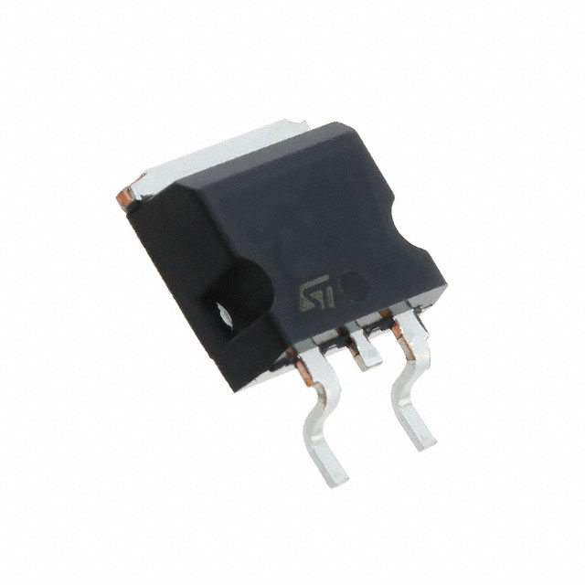
STB18N60DM2

Why Choose Us?
Professional Platform
B2B & B2C purchasingDelivery at full speed
1-2 days deliveryWide variety
Original manufacturers365 days guarantee
Responsible quality
.png)


Tech Specifications
STB18N60DM2 Description
STB18N60DM2 Description
The STB18N60DM2 is a high-performance MOSFET N-CH 600V 12A D2PAK produced by STMicroelectronics. This device is designed to meet the demands of modern electronics applications that require high voltage and current capabilities. With its advanced MOSFET technology, the STB18N60DM2 offers superior performance and reliability.
STB18N60DM2 Features
- 600V Drain to Source Voltage (Vdss): The STB18N60DM2 can handle high voltage applications, making it suitable for power electronics and industrial control systems.
- 12A Continuous Drain Current (Id) @ 25°C: This MOSFET can handle high current loads, ensuring efficient power delivery and management in various applications.
- 295mOhm Rds On (Max) @ 6A, 10V: The low on-resistance of the STB18N60DM2 contributes to its high efficiency and minimal power loss.
- 5V Vgs(th) (Max) @ 250µA: The STB18N60DM2 has a low threshold voltage, which simplifies the design process and improves performance in low-voltage applications.
- 20 nC Gate Charge (Qg) (Max) @ 10V: This low gate charge helps reduce switching losses and improve the overall efficiency of the device.
- 800 pF Input Capacitance (Ciss) (Max) @ 100 V: The STB18N60DM2 has a low input capacitance, which contributes to faster switching speeds and reduced power consumption.
- 90W Power Dissipation (Max): The device can handle high power dissipation, making it suitable for high-power applications.
- 150°C Operating Temperature (TJ): The STB18N60DM2 can operate in harsh environments with high temperatures, ensuring reliable performance in various applications.
- ROHS3 Compliant: The STB18N60DM2 meets environmental regulations, making it an eco-friendly choice for electronics manufacturers.
STB18N60DM2 Applications
The STB18N60DM2 is ideal for a wide range of applications due to its high voltage and current capabilities, low on-resistance, and low gate charge. Some specific use cases include:
- Power Electronics: The STB18N60DM2 can be used in power supplies, converters, and inverters, where high voltage and current handling are required.
- Industrial Control Systems: This MOSFET is suitable for motor drives, robotics, and other industrial applications that demand high power and reliability.
- Automotive Electronics: The STB18N60DM2 can be used in electric vehicle charging systems, battery management systems, and other high-voltage automotive applications.
- Renewable Energy Systems: This MOSFET is ideal for solar inverters, wind power systems, and other renewable energy applications that require high voltage and current capabilities.
Conclusion of STB18N60DM2
The STB18N60DM2 is a high-performance MOSFET that offers superior technical specifications and performance benefits over similar models. Its unique features, such as low on-resistance, low gate charge, and high power dissipation, make it an ideal choice for a wide range of applications in power electronics, industrial control systems, automotive electronics, and renewable energy systems. The STB18N60DM2's compliance with environmental regulations and its ability to operate in harsh environments further enhance its appeal to electronics manufacturers and engineers.
FAQ
| Quantity | Unit Price | Ext. Price |
|---|---|---|
| 1+ | $6.30857 | $6.31 |
| 10+ | $5.44115 | $54.41 |
| 30+ | $4.92515 | $147.75 |
Not available to buy online? Want the lower wholesale price? Please Send RFQ to get best price, we will respond immediately


.png?x-oss-process=image/format,webp/resize,h_32)


