
 German
 Japanese
 Portuguese
 Korea
Korea
 Mexico
 Dutch
Dutch


STMicroelectronics
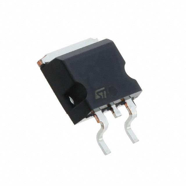
STB6N80K5

Why Choose Us?
Professional Platform
B2B & B2C purchasingDelivery at full speed
1-2 days deliveryWide variety
Original manufacturers365 days guarantee
Responsible quality
.png)


Tech Specifications
STB6N80K5 Description
STB6N80K5 Description
The STB6N80K5 is a high-performance N-Channel MOSFET from STMicroelectronics, designed for applications requiring high voltage and current handling capabilities. This device features a SuperMESH5™ series, which offers superior performance in terms of on-resistance and switching speed. With a drain-to-source voltage of 800V and a continuous drain current of 4.5A at 25°C, the STB6N80K5 is well-suited for various power electronics applications.
STB6N80K5 Features
- High Voltage and Current Handling: The STB6N80K5 can handle drain-to-source voltages up to 800V and continuous drain currents of 4.5A at 25°C, making it ideal for high-power applications.
- Low On-Resistance: The device features a maximum on-resistance of 1.6Ω at 2A drain current and 10V gate-source voltage, ensuring efficient power dissipation.
- Fast Switching Speed: With a maximum gate charge of 7.5nC at 10V gate-source voltage, the STB6N80K5 offers fast switching capabilities, reducing power losses in switching applications.
- Robust Package: The device is available in a D2PAK package, providing excellent thermal performance and mechanical stability.
- Environmental Compliance: The STB6N80K5 is REACH unaffected and RoHS3 compliant, ensuring compliance with environmental regulations.
STB6N80K5 Applications
The STB6N80K5 is well-suited for a variety of high-power applications, including:
- Power Supplies: Due to its high voltage and current handling capabilities, the STB6N80K5 is ideal for use in power supply designs, such as SMPS (Switched-Mode Power Supplies) and DC-DC converters.
- Motor Control: The device's fast switching speed and low on-resistance make it suitable for motor control applications, including electric vehicles, industrial drives, and robotics.
- Renewable Energy: The STB6N80K5 can be used in renewable energy systems, such as solar inverters and wind power converters, where high voltage and current handling are required.
Conclusion of STB6N80K5
The STB6N80K5 is a powerful N-Channel MOSFET from STMicroelectronics, offering a combination of high voltage and current handling capabilities, low on-resistance, and fast switching speed. Its robust D2PAK package and environmental compliance make it an ideal choice for a wide range of high-power applications, including power supplies, motor control, and renewable energy systems. With its unique features and advantages over similar models, the STB6N80K5 is a reliable and efficient solution for demanding power electronics applications.
FAQ
| Quantity | Unit Price | Ext. Price |
|---|---|---|
| 1+ | $1.98685 | $1.99 |
| 10+ | $1.94400 | $19.44 |
| 30+ | $1.91485 | $57.45 |
Not available to buy online? Want the lower wholesale price? Please Send RFQ to get best price, we will respond immediately


.png?x-oss-process=image/format,webp/resize,h_32)


