
STMicroelectronics
STWA20N95K5
Single FETs, MOSFETs


.png?x-oss-process=image/format,webp/resize,p_30)


STWA20N95K5 Description
STWA20N95K5 Description
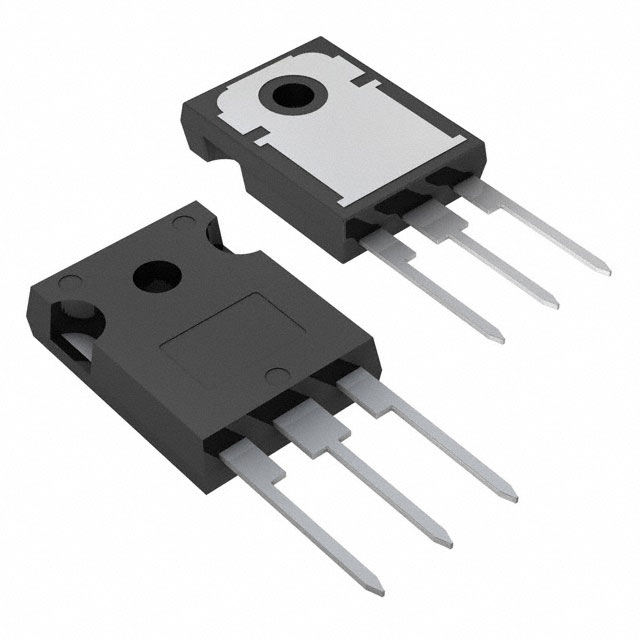
The STWA20N95K5 from STMicroelectronics is a high-performance N-channel MOSFET designed for demanding power applications. With a 950V drain-to-source voltage (Vdss) and 17.5A continuous drain current (Id), this device is optimized for efficiency and reliability in high-voltage circuits. It features SuperMESH5™ technology, which significantly reduces on-state resistance (Rds(on) of 330mΩ @ 9A, 10V) while maintaining low gate charge (Qg(max) of 40nC @ 10V). Packaged in a TO-247 through-hole format, it ensures robust thermal performance with a maximum power dissipation of 250W (Tc).
STWA20N95K5 Features
- High Voltage Rating: 950V Vdss for industrial and automotive applications.
- Low Rds(on): 330mΩ minimizes conduction losses, improving efficiency.
- SuperMESH5™ Technology: Enhances switching performance and reduces energy losses.
- Low Gate Charge (Qg): 40nC ensures faster switching speeds and lower drive requirements.
- High Power Handling: 250W dissipation capability for thermally challenging environments.
- Robust Construction: TO-247 package offers superior thermal management.
- Compliance: ROHS3, REACH unaffected, and ECCN EAR99 certified for global use.
STWA20N95K5 Applications
This MOSFET is ideal for:
- Switch-mode power supplies (SMPS) in industrial and telecom systems.
- Motor drives and inverters requiring high-voltage switching.
- Renewable energy systems, such as solar inverters and wind power converters.
- Automotive applications, including EV charging and traction control.
- High-voltage DC-DC converters where efficiency and reliability are critical.
Conclusion of STWA20N95K5
The STWA20N95K5 stands out as a high-efficiency, high-voltage MOSFET with SuperMESH5™ technology, making it a superior choice for power electronics. Its low Rds(on), high current capability, and robust thermal performance ensure reliability in demanding applications. Whether for industrial, automotive, or renewable energy systems, this device delivers optimal performance, reduced losses, and long-term durability. Its compliance with global standards further enhances its suitability for diverse markets.
Tech Specifications
STWA20N95K5 Documents
Download datasheets and manufacturer documentation for STWA20N95K5
 IPD/15/9124 20/Mar/2015
  STWA20N95K5
  STWA20N95K5
 Shopping Guide


.png?x-oss-process=image/format,webp/resize,h_32)


