
STMicroelectronics
STP5N60M2
Single FETs, MOSFETs


.png?x-oss-process=image/format,webp/resize,p_30)


STP5N60M2 Description
STP5N60M2 Description
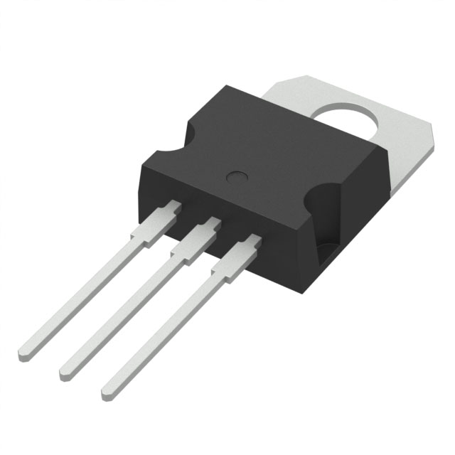
The STP5N60M2 is a high-performance MOSFET (Metal Oxide) from STMicroelectronics, designed for a wide range of applications in the electronics industry. With a drain-source voltage of 600V and a continuous drain current of 3.7A at 25°C, this N-channel MOSFET offers excellent performance and reliability. It is manufactured using advanced technology and is compliant with RoHS3 standards, making it an environmentally friendly choice.
STP5N60M2 Features
- High Voltage and Current Ratings: The STP5N60M2 can handle a drain-source voltage of up to 600V and a continuous drain current of 3.7A at 25°C, making it suitable for high-power applications.
- Low On-Resistance: With a maximum on-resistance of 1.4Ω at 1.85A and 10V, the STP5N60M2 offers low power dissipation and high efficiency.
- Robust Gate Drive: The device has a maximum gate-source voltage of ±25V, ensuring reliable operation in various gate drive conditions.
- Low Gate Charge: The maximum gate charge is 4.5nC at 10V, which contributes to faster switching speeds and reduced power loss.
- REACH Unaffected: The STP5N60M2 is not affected by REACH regulations, ensuring compliance with environmental standards.
- Moisture Sensitivity Level 1: With an MSL of 1, the device can be stored and handled without special precautions, simplifying the manufacturing process.
- Wide Operating Temperature Range: The STP5N60M2 operates at a junction temperature of up to 150°C, making it suitable for high-temperature applications.
STP5N60M2 Applications
The STP5N60M2 is ideal for various applications where high voltage and current handling capabilities are required. Some specific use cases include:
- Power Supplies: The high voltage and current ratings make the STP5N60M2 suitable for power supply applications, such as switching power supplies and battery chargers.
- Motor Control: The low on-resistance and robust gate drive characteristics make it an excellent choice for motor control applications, including brushless DC motors and stepper motors.
- Industrial Automation: The STP5N60M2's high performance and reliability make it suitable for industrial automation applications, such as robotic arms and conveyor systems.
- Automotive Applications: The device's high voltage and current ratings, along with its wide operating temperature range, make it suitable for automotive applications, such as electric vehicle chargers and power electronics.
Conclusion of STP5N60M2
The STP5N60M2 is a versatile and high-performance MOSFET from STMicroelectronics, offering excellent technical specifications and performance benefits. Its unique features, such as low on-resistance, low gate charge, and high voltage and current ratings, make it an ideal choice for a wide range of applications in the electronics industry. With its compliance with environmental standards and robust performance, the STP5N60M2 is a reliable and efficient solution for high-power applications.
Tech Specifications
STP5N60M2 Documents
Download datasheets and manufacturer documentation for STP5N60M2
 STx5N60M2
  STx5N60M2
 Shopping Guide


.png?x-oss-process=image/format,webp/resize,h_32)


