
STMicroelectronics
STW45N60DM2AG
Single FETs, MOSFETs


.png?x-oss-process=image/format,webp/resize,p_30)


STW45N60DM2AG Description
STW45N60DM2AG Description
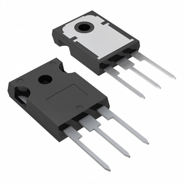
The STW45N60DM2AG is a high-performance N-Channel MOSFET from STMicroelectronics, designed for automotive applications. It features a 600V drain-to-source voltage rating and a continuous drain current of 34A at 25°C, making it suitable for a wide range of power electronics applications. The device is manufactured using advanced MOSFET technology, ensuring high efficiency and reliability.
STW45N60DM2AG Features
- 600V Drain-to-Source Voltage (Vdss): Provides robust voltage handling capabilities for various power electronics applications.
- 34A Continuous Drain Current (Id) @ 25°C: Delivers high current capacity for demanding power management tasks.
- 93mOhm Rds On (Max) @ 17A, 10V: Offers low on-resistance for efficient power dissipation.
- 5V Vgs(th) (Max) @ 250µA: Ensures low gate drive voltage requirements for ease of use in various circuits.
- 2500 pF Input Capacitance (Ciss) (Max) @ 100 V: Minimizes parasitic effects and improves high-frequency performance.
- 56 nC Gate Charge (Qg) (Max) @ 10 V: Reduces switching losses and improves efficiency.
- ±25V Vgs (Max): Allows for a wide range of gate voltage compatibility.
- 250W Power Dissipation (Max): Enables high power handling capabilities.
- Automotive Grade: Designed to meet the stringent requirements of automotive applications.
- Through Hole Mounting Type: Facilitates easy integration into existing designs.
STW45N60DM2AG Applications
The STW45N60DM2AG is ideal for a variety of high-power, high-voltage applications in the automotive sector, including:
- Battery Management Systems: Manages power flow between the battery and various vehicle systems.
- DC-DC Converters: Converts voltage levels for efficient power distribution.
- Motor Controls: Drives electric motors in electric and hybrid vehicles.
- Power Supplies: Provides stable power to various automotive electronics.
Conclusion of STW45N60DM2AG
The STW45N60DM2AG from STMicroelectronics is a powerful, reliable N-Channel MOSFET designed for demanding automotive applications. Its high voltage and current ratings, combined with low on-resistance and gate charge, make it an excellent choice for power electronics designs. With its automotive-grade rating and through-hole mounting, the STW45N60DM2AG is a versatile solution for a wide range of high-power applications.
Tech Specifications
STW45N60DM2AG Documents
Download datasheets and manufacturer documentation for STW45N60DM2AG
 Mult Dev Assembly Chg 19/Dec/2018
  STW45N60DM2AG
  Standard outer labelling 15/Nov/2023
  STW45N60DM2AG
 Shopping Guide


.png?x-oss-process=image/format,webp/resize,h_32)


