

STMicroelectronics
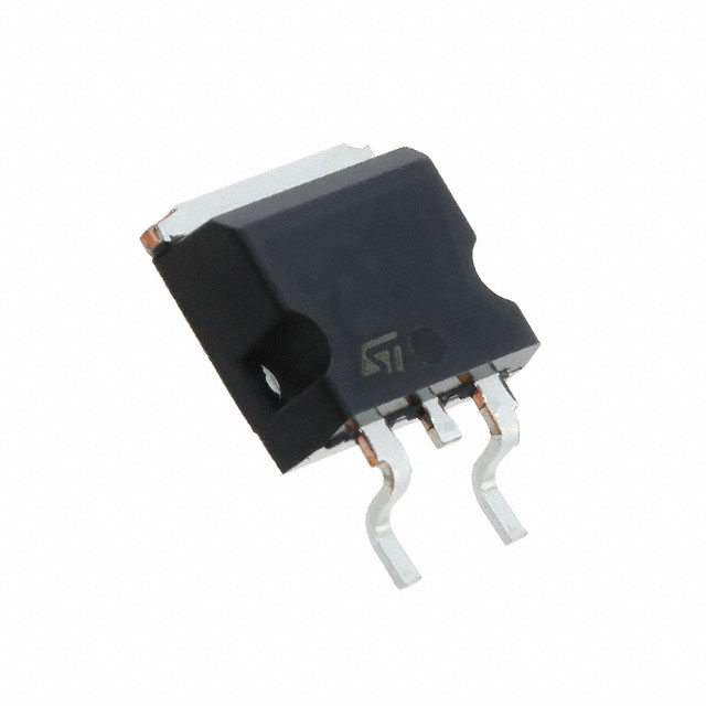
STB45N50DM2AG
Single FETs, MOSFETs

Not available to buy online? Want the lower wholesale price? Please Send RFQ to get best price, we will respond immediately


.png?x-oss-process=image/format,webp/resize,p_30)


STB45N50DM2AG Description
STB45N50DM2AG Description
The STB45N50DM2AG is a high-performance N-channel MOSFET from STMicroelectronics, designed for automotive applications. This device is part of the MDmesh™ DM2 series and offers exceptional performance in terms of power dissipation, voltage handling, and current capacity. With a drain-to-source voltage (Vdss) of 500V, it can handle high-voltage applications with ease. The device is surface-mountable, making it ideal for compact designs and high-density packaging.
STB45N50DM2AG Features
- High Drain-to-Source Voltage (Vdss): 500V, suitable for high-voltage applications.
- Power Dissipation (Max): 250W (Tc), ensuring efficient heat management.
- Current - Continuous Drain (Id) @ 25°C: 35A (Tc), providing high current capacity.
- Low Rds On (Max) @ Id, Vgs: 84mOhm @ 17.5A, 10V, contributing to low power loss.
- Gate Charge (Qg) (Max) @ Vgs: 57 nC @ 10V, enabling fast switching.
- Input Capacitance (Ciss) (Max) @ Vds: 2600 pF @ 100 V, reducing parasitic effects.
- Vgs (Max): ±25V, providing robust gate voltage handling.
- Technology: MOSFET (Metal Oxide), ensuring reliability and longevity.
- Mounting Type: Surface Mount, suitable for compact and high-density designs.
STB45N50DM2AG Applications
The STB45N50DM2AG is ideal for a variety of high-voltage and high-current applications in the automotive industry. Some specific use cases include:
- Power Management Systems: Due to its high power dissipation and current capacity, it is suitable for managing power in vehicles.
- Battery Management Systems: The device's high voltage and current ratings make it ideal for managing battery charging and discharging.
- Electric Vehicle (EV) Components: Its high voltage and current ratings, along with its automotive-grade design, make it suitable for EV components such as motor controllers and inverters.
Conclusion of STB45N50DM2AG
The STB45N50DM2AG is a powerful and reliable MOSFET designed for high-voltage and high-current automotive applications. Its unique combination of high Vdss, low Rds On, and high Id, along with its automotive-grade features, make it an excellent choice for demanding applications where performance and reliability are critical. With its robust design and compliance with industry standards, the STB45N50DM2AG stands out as a top choice for engineers looking to push the boundaries of automotive electronics.
Tech Specifications
STB45N50DM2AG Documents
Download datasheets and manufacturer documentation for STB45N50DM2AG
Product Change Notification 2024-03-05 (PDF) Product Change Notification (PDF) PRODUCT CHANGE NOTIFICATION (PDF) Related Parts


Shopping Guide


.png?x-oss-process=image/format,webp/resize,h_32)


©2025 ERSA Electronics Corporation.