
STMicroelectronics
STW45N65M5
Single FETs, MOSFETs


.png?x-oss-process=image/format,webp/resize,p_30)


STW45N65M5 Description
STW45N65M5 Description
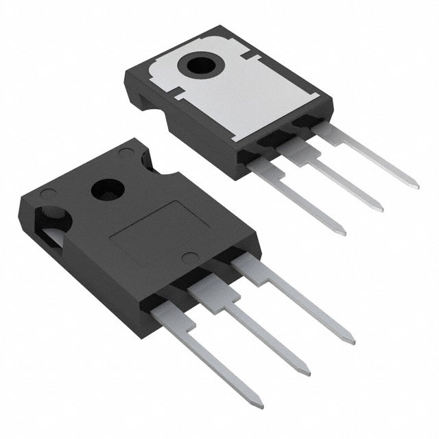
The STW45N65M5 is a powerful MOSFET (Metal Oxide) device manufactured by STMicroelectronics, designed for high-performance applications. This N-Channel device offers a drain-to-source voltage (Vdss) of 650V and can handle a continuous drain current (Id) of 35A at 25°C. With a maximum power dissipation of 210W and an operating temperature of 150°C, the STW45N65M5 is ideal for demanding applications.
STW45N65M5 Features
- High Voltage and Current Handling: The STW45N65M5 can handle a drain-to-source voltage of 650V and a continuous drain current of 35A, making it suitable for high-power applications.
- Low On-Resistance: With an Rds(on) of just 78mOhm at 19.5A and 10V, the STW45N65M5 offers low power dissipation and high efficiency.
- Robust Gate Drive: The device has a maximum gate-source voltage (Vgs) of ±20V and a threshold voltage (Vgs(th)) of 5V at 250µA, ensuring reliable operation.
- Low Input Capacitance: The STW45N65M5 has a maximum input capacitance (Ciss) of 3375pF at 100V, reducing switching losses and improving efficiency.
- Environmental Compliance: The device is REACH unaffected and RoHS3 compliant, ensuring environmental safety and regulatory compliance.
- Moisture Sensitivity Level (MSL) 1: The STW45N65M5 has an MSL of 1, indicating unlimited storage time before reflow soldering, simplifying logistics and inventory management.
STW45N65M5 Applications
The STW45N65M5 is ideal for a wide range of applications, including:
- Industrial Motor Control: The high voltage and current ratings make it suitable for motor drives and control systems.
- Power Supplies: The low on-resistance and high voltage capabilities make it an excellent choice for power supply designs.
- Automotive Applications: The device's robustness and temperature range make it suitable for automotive electronics, such as electric vehicle charging systems and power management.
- Renewable Energy Systems: The STW45N65M5 can be used in solar inverters and wind turbine power electronics, thanks to its high voltage and current ratings.
Conclusion of STW45N65M5
The STW45N65M5 from STMicroelectronics is a high-performance MOSFET designed for demanding applications requiring high voltage and current handling. Its low on-resistance, robust gate drive, and environmental compliance make it an excellent choice for industrial motor control, power supplies, automotive electronics, and renewable energy systems. With its unique features and advantages, the STW45N65M5 stands out among similar models, offering a reliable and efficient solution for high-power applications.
Tech Specifications
STW45N65M5 Documents
Download datasheets and manufacturer documentation for STW45N65M5
 IPG-PWR/14/8674 02/Sep/2014
  STW(A)45N65M5, STFW45N65M5
  Standard outer labelling 15/Nov/2023
  STW45N65M5 View All Specifications
  STW(A)45N65M5, STFW45N65M5
 Shopping Guide


.png?x-oss-process=image/format,webp/resize,h_32)


