
STMicroelectronics
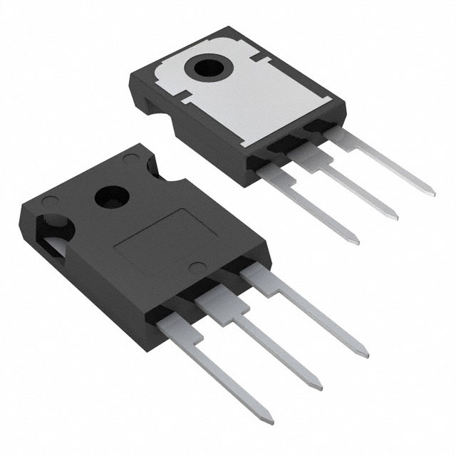
STWA50N65DM2AG
Single FETs, MOSFETs


.png?x-oss-process=image/format,webp/resize,p_30)


STWA50N65DM2AG Description
STWA50N65DM2AG Description
The STWA50N65DM2AG is a high-performance N-Channel MOSFET from STMicroelectronics, designed for demanding automotive applications. This MOSFET is built on the advanced MDmesh™ DM2 series, ensuring superior performance and reliability. With a drain-to-source voltage rating of 650V and a continuous drain current of 38A at 25°C, the STWA50N65DM2AG is capable of handling high-power applications efficiently.
STWA50N65DM2AG Features
- High Drain-to-Source Voltage (Vdss): 650V, making it suitable for high-voltage applications.
- Continuous Drain Current (Id): 38A at 25°C, ensuring robust current handling capabilities.
- Low Rds On: 87mOhm at 19A, 10V, contributing to high efficiency and low power loss.
- Gate Charge (Qg): 69nC at 10V, enabling fast switching and reduced switching losses.
- Input Capacitance (Ciss): 3200pF at 100V, providing fast response times.
- Maximum Gate-to-Source Voltage (Vgs): ±25V, offering flexibility in gate drive requirements.
- Automotive Grade: Designed to meet the stringent requirements of automotive applications.
- RoHS3 Compliant: Ensuring environmental compliance and sustainability.
- Moisture Sensitivity Level (MSL): 1, indicating unlimited storage time before reflow soldering.
STWA50N65DM2AG Applications
The STWA50N65DM2AG is ideal for a variety of high-power automotive applications, including:
- Electric Vehicle (EV) Inverters: Due to its high voltage and current ratings, it is well-suited for inverter applications in electric and hybrid vehicles.
- DC-DC Converters: Its low Rds On and high efficiency make it an excellent choice for DC-DC converters in automotive systems.
- Motor Controls: The STWA50N65DM2AG can be used in motor control applications, providing precise control and high efficiency.
- Power Management Systems: Its robust performance and automotive grade rating make it suitable for power management in various automotive systems.
Conclusion of STWA50N65DM2AG
The STWA50N65DM2AG from STMicroelectronics stands out as a high-performance, automotive-grade MOSFET. Its unique combination of high voltage and current ratings, low Rds On, and fast switching capabilities make it an excellent choice for demanding automotive applications. Its compliance with RoHS3 and REACH standards, along with its moisture sensitivity level, further enhance its appeal for environmentally conscious and reliability-focused designs. The STWA50N65DM2AG is a powerful component for engineers looking to push the boundaries of performance and efficiency in their automotive projects.
Tech Specifications
STWA50N65DM2AG Documents
Download datasheets and manufacturer documentation for STWA50N65DM2AG
 Wafer 15/Feb/2019
  STWA50N65DM2AG
 Shopping Guide


.png?x-oss-process=image/format,webp/resize,h_32)


