
 German
 Japanese
 Portuguese
 Korea
Korea
 Mexico
 Dutch
Dutch


Open-Cavity (Open-Lid) IC Packages: Air-Cavity QFN for Prototyping & Optics

A chip open lid package is an open-cavity IC package that exposes the die for bonding, optical alignment, or RF tuning, then optionally seals with a ceramic or metal lid; engineers use it for prototyping and validation while keeping a QFN-compatible footprint.
Direct heat path to heatsink
Die access for bonding/optics
QFN-compatible; easy migration

What is Open-Cavity / Open-Lid IC Packaging?
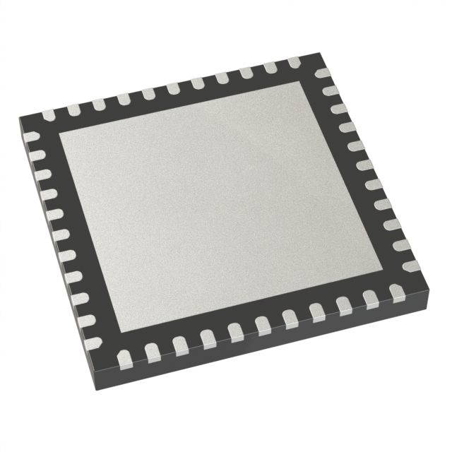
A chip open lid package is an open-cavity IC package shipped with the lid removed (or only partially attached) so engineers can access the die for bonding, optical alignment, debug, or RF tuning. After evaluation, the device may be sealed with a metal or ceramic lid using epoxy or glass-frit, or it can remain open depending on the application. In practice, the terms open-lid package, open-cavity package, and air-cavity QFN describe the same family of packages that preserve QFN/QFP-style footprints while exposing the cavity during engineering builds.
- open-lid / open-cavity — common industry wording for lid-removed or lid-ready packages.
- air-cavity QFN/QFP — cavity above the die; many variants are footprint-compatible with plastic QFN/QFP.
- Lid & sealing — metal or ceramic lids; epoxy or glass-frit attach depending on thermal, process, and reliability targets.
Relation to interconnect styles: open-lid/open-cavity describes the package form, while wire-bond and flip-chip describe the die interconnect. Open-cavity packages commonly support wire-bond for visibility and rework, and can also be combined with flip-chip (bumps/copper pillars) when high I/O density and short interconnect paths are required.

Flip-Chip Background
Flip-chip is an interconnect approach where the die’s active face is turned toward the substrate and joined through solder bumps or copper pillars, minimizing the electrical path versus wire bonding. In a flip-chip package, these short connections reduce parasitics, enable high-density routing, and unlock higher-bandwidth I/O. For this page’s topic—open-lid / open-cavity packaging—flip-chip is orthogonal to the package form: engineers may pair it with an open lid to keep die access for thermal contact or inspection while retaining flip-chip’s electrical advantages. Conversely, many engineering builds still use wire-bond in open-cavity variants for visibility and easy rework.
- RDL → bumps/pillars → underfill: short, low-inductance paths with controlled impedance.
- High-density routing: more I/O in smaller footprints; better escape routing on the substrate.
- High-speed links: improved signal integrity for SerDes and other multi-Gbps interfaces.
| Dimension | Flip-Chip | Wire-Bond |
|---|---|---|
| I/O density | Very high (area array) | Moderate (periphery) |
| Signal speed / path length | Short path, higher bandwidth | Longer loop, more parasitics |
| Routing density | Dense escape & multilayer fan-out | Less dense; perimeter-limited |
| Rework / visibility | Harder to probe/repair | Easier visual access & re-bond |
| Typical pairing with open-lid | When density/speed dominate | When visibility/rework dominate |
Choose flip-chip + open-lid when your design demands high I/O density and multi-Gbps links yet still benefits from die-level thermal contact or visual inspection. Prefer wire-bond + open-cavity for maximum visibility, quick rework, and cost-sensitive engineering builds.

Explore related topics: Interface ICs and High-speed / SerDes (USB 3.0 guide).
Continue with foundational topics: SMD Components and PCB Layout Design.
Open-Lid Configurations
In a chip open lid package (also called open-lid / open-cavity or air-cavity QFN), three practical configurations are used to balance thermal path, protection, and operability: lidless, flat-lidded (partial), and fully lidded. The choice drives how directly the die can touch a heatsink, how easy probing/rework remains, and how much environmental protection the package provides.
Lidless
Backside fully exposed → best thermal path, supports direct heatsink contact.
Trade-off: higher assembly/ESD/contamination risk; strict process control required.
Flat-Lidded / Partial Lid
Partially covered or non-hermetic lid → some protection while retaining thermal path and limited die access; good for engineering builds.
Fully Lidded
Completely sealed lid → maximum protection and heat spreading, but less convenient for later probing or rework; closer to production practice.
| Dimension | Lidless | Flat-Lidded / Partial | Fully Lidded |
|---|---|---|---|
| Footprint / Size | Often QFN-compatible; minimal z-height | QFN-compatible; lid adds modest height | QFN/QFP-style; highest z-height |
| Thermal Path | Direct die-to-heatsink contact | Mixed: lid + cavity conduction | Spreading via lid; indirect path |
| Operability (Probe/Rework) | Best visibility; easiest access | Limited access; planned windows | Minimal; de-lid needed |
| Reliability Envelope | Sensitive to moisture/contamination | Balanced; depends on lid attach | Highest protection; stress control |
| Assembly Risk | High (ESD, handling, cleanliness) | Medium (seal alignment/process) | Medium–Low (repeatable sealing) |
| Typical Use-Cases | RF tuning, optical alignment, FA | Engineering builds, limited debug | Pre-production, reliability trials |

Prioritize lidless for direct thermal contact and maximum probe access; choose partial-lid for a balance of protection and debugging; use fully lidded when approaching production and reliability screening.
See related build notes in PCB Layout Design and explore power-dense use cases in Power Management ICs.
Benefits & Trade-offs
In a chip open lid package—also called an open-lid package, open-cavity package, or air-cavity QFN—you trade among thermal performance, operability (probing/rework), and protection. This section outlines when the headline benefits really apply and what risks to control during design and assembly.
Improved thermal performance
When it applies: lidless or partial-lid builds that allow direct contact to a heatsink or a shorter thermal path— especially for power-dense PMICs and RF front ends. Note: control flatness/co-planarity and exposed-pad (EP) contact area to avoid hot spots.
Potential size reduction
When it applies: height-constrained designs where removing the lid stack lowers z-height, or optics that need tight alignment space. Note: verify mechanical protection and ESD strategy when the die is more exposed.
Cost optimization
When it applies: engineering phases that benefit from faster rework and fewer de-lid cycles, while keeping a plastic-QFN-compatible footprint for later migration. Note: ceramic/metal lids and glass-frit sealing can raise unit cost in samples; total program cost often still drops via quicker turns.
Trade-offs & Risks
- Handling & Assembly: exposed die is fragile; higher ESD class; probe/fixture scratches; strict cleanliness and dedicated tooling.
- Thermal Management: TIM selection (viscosity, pump-out, thickness), flatness/co-planarity, EP via array design, and lid-attach stress (CTE mismatch).
- Environmental Protection: MSL handling, moisture/ionic contamination, cavity cleanliness, outgassing (optics/RF impact), and post-seal leakage (if hermeticity matters).
Engineering Checklist

Explore power-dense use cases in Power Management ICs and material choices in PCB Materials / Stackup.
IC Types & Real Use Cases
In a chip open lid package (aka open-lid / open-cavity or air-cavity QFN), the following IC categories commonly leverage direct die access, shorter thermal paths, and flexible sealing. Each module below includes a recommended configuration, typical companion ICs, a migration tip, and a soft CTA for BOM submission or browsing related parts.

MEMS Sensors (Accelerometer / Gyro / Pressure)
Engineering builds benefit from calibration/trim visibility and direct access to the die and bond area. Open cavities also make it easier to control cavity cleanliness and verify wire-bond loops under a microscope during bring-up. For inertial/pressure MEMS, the learning cycle on yield and drift is faster when the package remains accessible.
Recommended configuration: Partial-lid for balanced protection + access; lidless when tight alignment or thermal contact is required.
Companion ICs: Precision AFE/ADC, Interface (I²C/SPI), PMIC (LDO/Buck).
Migration tip: keep land pattern/EP identical to the plastic QFN target; validate reflow + temperature cycling.
Optical Devices & Drivers (Photodiode / VCSEL / Laser)
Optical modules need alignment windows and ultra-clean cavities; outgassing and residues directly impact SNR and optical power. Open-lid builds allow precise die-to-optics alignment and thermal contact for stable power control during tests.
Recommended configuration: Lidless for alignment and heat; migrate to partial/full-lid before reliability screening.
Companion ICs: Laser/LED drivers, Transimpedance AFE, high-speed clock/SerDes.
Migration tip: re-check lid-attach temperature/stress and optical window tolerances when sealing (epoxy vs glass-frit).
RF Front-End / PA Modules
RF prototypes benefit from cavity tuning and direct thermal paths for high dissipation. Keeping the cavity open eases component swaps, matching tweaks, and thermal interface experiments before locking the production stack.
Recommended configuration: Lidless for the best heat path; partial-lid when structural robustness is needed.
Companion ICs: PA/FE modules, RF switches, PMIC (buck/boost), telemetry interfaces.
Migration tip: revisit EP via arrays, TIM, and parasitic changes when shifting to plastic QFN; re-run RF validation.
High-Fidelity Analog Front-Ends / Test MCUs
Lab cycles often require frequent probing and rework. Open cavities simplify noise-path validation on AFEs and pin-function validation on MCUs, while keeping the QFN footprint compatible with production targets.
Recommended configuration: Partial-lid for balanced protection and access; lidless in controlled labs.
Companion ICs: Precision AFE/ADC, timing/clock, Interface (USB/Serial), PMIC.
Migration tip: translate bench probe/test points to DFT/ICT for volume; re-qualify thermal, reflow, and reliability.
| Use Case | Recommended Configuration | Companion ICs (PMIC/AFE/Interface) | Migration Notes |
|---|---|---|---|
| MEMS Sensors | Partial-lid; lidless for alignment | AFE/ADC, I²C/SPI, PMIC | Match plastic QFN footprint; validate reflow & TC |
| Optical Devices | Lidless → Partial/Full-lid before qual | Laser driver, TIA, SerDes | Re-check seal temps/stress; window tolerance |
| RF Front-End / PA | Lidless; Partial for robustness | PA/FE, RF switch, PMIC | Revisit EP vias, TIM; re-run RF validation |
| Analog AFE / Test MCUs | Partial-lid; Lidless in lab | Precision AFE/ADC, USB/Serial, PMIC | Map probes → DFT/ICT; re-qualify thermal/reflow/reliability |
Design & Assembly Notes
For open-cavity / open-lid builds, success hinges on disciplined PCB footprinting and keep-outs, a verified thermal path, strict cleanliness, controlled reflow, thorough inspection, and reliability re-qualification. Always reconcile your CAD with the supplier’s package drawing and STEP model before release.
PCB Footprint
- Land pattern & EP: match pad/EP dimensions and co-planarity to the drawing; validate with 2D + STEP.
- Lid overhang keep-out: reserve mechanical space around the package for lid overhang and tooling; avoid tall-neighbor clashes.
- Solder-mask strategy: fine pitch pins may prefer SMD; align EP mask window and annular rings to paste spread.
- Silkscreen: keep legends away from EP and the cavity/window region; protect fiducials.
- Stencil: use EP segmented apertures to curb float; consider corner-relief reductions on pin apertures.
- Final authority: vendor package drawing + formal DFM review.
Thermal
- EP via array: dense, even vias under EP; choose tented/plugged/filled per process and cleanliness plan.
- TIM selection: grease/pad/PCM—check compressibility, pump-out, and thickness control vs. flatness/co-planarity.
- Heatsink contact: ensure adequate area, surface roughness, and pressure distribution to avoid die bowing.
- Path consistency: expect Rθ and spreading to change when migrating to plastic QFN; re-model and re-measure.
Cleanliness
- MSL & bake: follow label/vendor guidance; open cavities are more moisture-sensitive.
- Flux/residue: prevent residues entering the cavity; decide selective clean vs. no-clean per chemistry.
- N2 protection: use nitrogen during lid attach or critical reflow stages to reduce oxidation and residue hardening.
- Handling/tooling: fixtures/probes must avoid scratching exposed areas; align to the required ESD class.
Reflow
- Two profiles: validate pre-lid and post-lid profiles; epoxy/glass-frit cure temperatures can shift stress.
- Thermal window: respect vendor peak/soak/ramps; avoid cavity “popcorn” from trapped volatiles.
- Tooling/support: mitigate large-EP warpage; protect the exposed die/bond loops from compression.
Inspection
- C-SAM / AXI: check die-attach/EP voids before and after lid attach; confirm bond-area uniformity.
- Visual/microscopy: verify cavity particles, residues, scratches, and window cleanliness.
- Leak testing: perform gross/fine leak only if hermetic specifications apply.
Reliability
- CTE mismatch: account for lid (metal/ceramic) vs. substrate/silicon expansion; identify stress hot spots.
- Re-qualification: temperature cycling, HTOL/THB, and drop—before migrating to volume plastic packages.
- Reflow stress check: monitor parameter drift after multiple reflows and power-on cycles.
Engineering Quick Checklist

See also PCB Layout Design, SMD Components, and Reflow Profile.
Migration to Plastic QFN
Many teams prototype with a chip open lid package for debug and thermal bring-up, then migrate to plastic QFN for volume. Migration is not a copy-paste: materials, heat spreading, reflow windows, and reliability thresholds change. Use the steps below to lock the footprint, re-calibrate thermal behavior, re-verify process windows, and re-qualify reliability before SOP.
Footprint Lock
- Land pattern / EP: 100% match target plastic QFN pads, EP size, mask openings, and stencil regions.
- Height / Keep-out: verify z-height deltas vs. open-lid builds; check neighbor and heatsink clearances.
- Panelization & copper: include panel layout and copper balance (thieving) in DFM early.
- Documentation: freeze 2D drawing + STEP revs; define ECO triggers for any footprint change.
Thermal Re-Calibration
- Material shift: molding compound vs. metal/ceramic lids changes spreading; rebuild + measure RθJA / RθJC.
- TIM/contact: if lidless direct-contact was used, re-tune TIM choice, surface finish, and clamp pressure for plastic QFN.
- Measurement: thermocouples + IR; reproduce step-power profiles and worst-case duty cycles.
- EP vias: confirm via array / fill strategy still meets volume thermal targets.
Reflow & Materials
- Profile swap: replace pre-/post-lid engineering profiles with the vendor’s plastic-QFN recommendation; verify peak/soak/ramps.
- MSL / Bake: reset bake rules and WIP time to the production MSL level.
- Flux / cleaning: re-assess no-clean vs. selective clean for residues on plastic packages.
- Warpage / support: re-validate fixturing for large EP parts on the volume line.
Reliability Re-Qualification
- J-STD-020 MSL (incl. 3× reflow) at production spec.
- Environmental: TCT (temp cycling), HTOL, THB/HAST per product class.
- Mechanical: drop / vibration / twist per standard.
- NDT: C-SAM / AXI re-check die-attach/EP voids after the package change.
- Pre-SOP sampling: align AQL and reject criteria with QA.
Project Milestones
EVT (Open-lid prototype)
- Key Deliverables
- Functional bring-up; thermal/probing; initial BOM
- Pass Criteria
- Basic performance met; risks logged
DVT (Plastic QFN engineering)
- Key Deliverables
- Thermal re-cal; reflow profile set; reliability matrix kicked off; DFM review
- Pass Criteria
- Profiles locked; thermal margins met; DFM sign-off
PVT (Pilot build)
- Key Deliverables
- Process parameters frozen; CP/QA reports; production doc pack
- Pass Criteria
- Yield at target; CTQs within control limits
SOP / Ramp
- Key Deliverables
- Monitor first 3 lots; ECN/ECO gates ready
- Pass Criteria
- Stable yield & field feedback; issue closure plan
Migration Checklist

Submit Your BOM / Migration Review
Downloadable Resources
Engineers working with a chip open lid package (open-lid / open-cavity, air-cavity QFN) can use these concise PDFs for design reviews, DFM checks, and migration planning.
Open-Cavity QFN Design & Integration Checklist (PDF)
PDF
One-page checklist covering footprint/EP, lid-overhang keep-outs, thermal path & TIM, MSL/cleanliness, and reflow/inspection essentials.
- Footprint/EP & lid-overhang keep-outs
- Thermal path & TIM checks
- MSL/bake & cleanliness controls
- Reflow / inspection / reliability quick list
Sealing Methods: Epoxy vs Glass-Frit for Open-Lid Packages (PDF)
PDF
Side-by-side comparison of epoxy and glass-frit lid attach: cure profiles, stress & CTE effects, hermeticity, residue/outgassing, and reworkability.
- Process flows & cure profiles
- Stress/CTE & reliability implications
- Hermeticity & residue/outgassing notes
- Selection guide by use case
Footprint Compatibility Guide: Air-Cavity QFN ↔ Plastic QFN (PDF)
PDF
Step-by-step mapping of land pattern, EP, stencil zoning, and keep-outs—plus thermal/reflow/reliability notes for a smooth migration path.
- Land/EP/stencil mapping checklist
- Lid-overhang vs plastic z-height
- EP via array & TIM adjustments
- Reflow & reliability notes before SOP
FAQs
Is “open-lid” the same as “open-cavity”?
Short answer: In engineering context, yes—both refer to packages shipped with the lid removed or partially attached to expose the die (often called a chip open lid package).
They enable access to bond areas and the cavity during bring-up and test, commonly seen as air-cavity QFN/QFP. See the definition in What is Open-Cavity / Open-Lid IC Packaging?
Can air-cavity QFN share the same PCB footprint with plastic QFN?
Usually yes, provided the land pattern, exposed pad (EP), and solder-mask openings match the supplier’s package drawing.
Also confirm lid overhang keep-out, EP via strategy, and stencil zoning; re-verify reflow and thermal when migrating. See Design & Assembly Notes, Migration, and download the Footprint Compatibility Guide (PDF).
When should I pick lidless vs partial-lid?
Pick lidless for direct heatsink contact, probing, or optical alignment; pick partial-lid when you need some protection but still want limited access.
High-power RF and optics prototypes often start lidless, then move to partial/full-lid for reliability. See Open-Lid Configurations and Benefits & Trade-offs.
What sealing method should I use: epoxy or glass-frit?
Epoxy offers flexible processing and friendlier rework; glass-frit runs hotter but can provide tighter stress control and hermeticity depending on design.
Choose by thermal/stress, cleanliness, and leak requirements, and validate cure profiles. See Epoxy vs Glass-Frit (PDF) and Reflow/Cleanliness notes.
How to manage cleanliness and outgassing risks?
Control MSL/bake and flux residues, use N2 on critical steps, and inspect under microscope; run C-SAM/AXI before and after sealing.
Optics/RF need tighter particle and volatile limits; add leak tests if required. See Design & Assembly Notes and the Design & Integration Checklist (PDF).
What reliability tests are recommended before migration?
Plan for TCT, HTOL, THB/HAST, and drop/vibration, plus J-STD-020 MSL re-validation including three reflows.
After switching package type, re-check thermal models and non-destructive inspections (C-SAM/AXI). See Migration to Plastic QFN or submit your BOM for a tailored plan.
Need Package Advice for Your Design?
Send your BOM or a photo list. We’ll suggest package matches, cross-brand alternates, and a migration plan from engineering samples to plastic QFN.
- Footprint/EP/stencil alignment for air-cavity ↔ plastic QFN
- Cross-brand alternatives and availability signal
- Thermal/reflow/reliability checklist before SOP

Related Articles
- ·HBM3E vs. HBM4: What Changes for Bandwidth, Interface Width, and Packaging
- ·HBM Explained: Why High-Bandwidth Memory Is Critical for AI Accelerators
- ·Beyond Capacity: Why Bandwidth and Power Efficiency Now Define Memory Value
- ·Understanding Memory Price Cycles: Key Drivers Behind Supply and Demand Shifts
- ·DRAM vs. NAND: How AI Demand Is Reshaping the Memory Industry
- ·HBM Explained: Why High-Bandwidth Memory Is Critical for AI Accelerators
- ·Beyond Capacity: Why Bandwidth and Power Efficiency Now Define Memory Value
- ·Understanding Memory Price Cycles: Key Drivers Behind Supply and Demand Shifts
- ·DRAM vs. NAND: How AI Demand Is Reshaping the Memory Industry
- ·Memory Chip Market Outlook: What Buyers Should Watch Heading into Q4





.png?x-oss-process=image/format,webp/resize,h_32)


