
STMicroelectronics
STF100N10F7
Single FETs, MOSFETs

Not available to buy online? Want the lower wholesale price? Please Send RFQ to get best price, we will respond immediately


.png?x-oss-process=image/format,webp/resize,p_30)


STF100N10F7 Description
STF100N10F7 Description
The STF100N10F7 is a high-performance N-channel MOSFET from STMicroelectronics, designed for applications requiring high voltage and current handling capabilities. With a drain-source voltage rating of 100V and continuous drain current of 45A at 25°C, this MOSFET is ideal for use in various power electronic applications. The device is manufactured using advanced MOSFET technology, ensuring high efficiency and reliability.
STF100N10F7 Features
- High Voltage and Current Ratings: The STF100N10F7 can handle drain-source voltages up to 100V and continuous drain currents up to 45A at 25°C, making it suitable for high-power applications.
- Low On-Resistance: With a maximum on-resistance of 8mΩ at 22.5A and 10V gate-source voltage, the STF100N10F7 offers low conduction losses, improving overall efficiency.
- High Input Capacitance: The device features a maximum input capacitance of 4369pF at 50V, providing fast switching performance.
- Low Gate Charge: The maximum gate charge is 61nC at 10V gate-source voltage, enabling fast switching and reducing power dissipation.
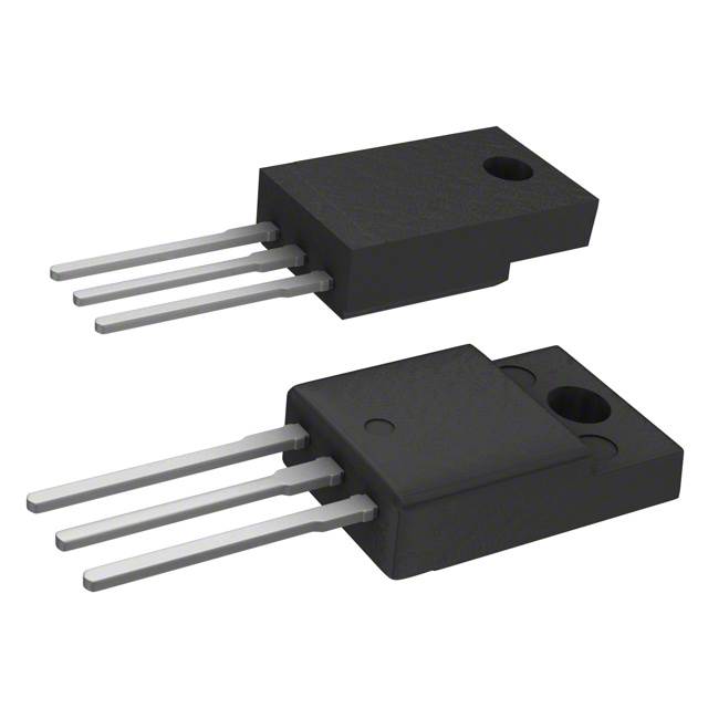
- Robust Package: The STF100N10F7 is packaged in a TO-220FP package, providing excellent thermal performance and mechanical robustness.
- Compliance with Regulations: The device is compliant with RoHS3 and REACH regulations, making it suitable for use in environmentally conscious applications.
STF100N10F7 Applications
The STF100N10F7 is ideal for a wide range of power electronic applications, including:
- Power Supplies: The high voltage and current ratings make it suitable for use in power supply designs, such as switch-mode power supplies (SMPS) and uninterruptible power supplies (UPS).
- Motor Control: The low on-resistance and fast switching capabilities make it an excellent choice for motor control applications, including electric vehicles (EVs) and industrial motor drives.
- Inverters: The STF100N10F7 can be used in inverter designs for renewable energy systems, such as solar and wind power inverters.
- Industrial Automation: The device's robustness and high performance make it suitable for use in industrial automation applications, such as servo drives and robotics.
Conclusion of STF100N10F7
The STF100N10F7 is a high-performance N-channel MOSFET from STMicroelectronics, offering a combination of high voltage and current ratings, low on-resistance, and fast switching capabilities. Its robust package and compliance with environmental regulations make it an excellent choice for a wide range of power electronic applications. With its advanced features and performance benefits, the STF100N10F7 is a reliable and efficient solution for demanding power electronic designs.
Tech Specifications
STF100N10F7 Documents
Download datasheets and manufacturer documentation for STF100N10F7
Assembly Site 03/Oct/2023 STx100N10F7 DataSheet STx100N10F7 DataSheet Related Parts


Shopping Guide


.png?x-oss-process=image/format,webp/resize,h_32)


©2025 ERSA Electronics Corporation.