
 German
 Japanese
 Portuguese
 Korea
Korea
 Mexico
 Dutch
Dutch


STMicroelectronics
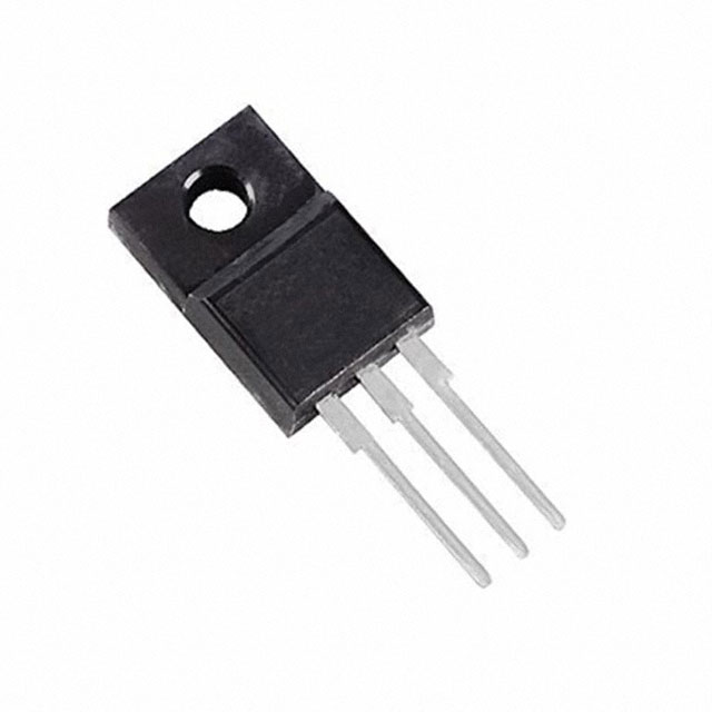
STF8N65M5

Why Choose Us?
Professional Platform
B2B & B2C purchasingDelivery at full speed
1-2 days deliveryWide variety
Original manufacturers365 days guarantee
Responsible quality
.png)


Tech Specifications
STF8N65M5 Description
STF8N65M5 Description
The STF8N65M5 is a high-performance MOSFET (Metal Oxide) from STMicroelectronics, designed for applications requiring high voltage and current capabilities. With a drain-source voltage (Vdss) of 650V and a continuous drain current (Id) of 7A at 25°C, this N-Channel device offers robust performance in various electronic systems.
STF8N65M5 Features
- High Voltage and Current Handling: The STF8N65M5 can handle a maximum drain-source voltage of 650V and a continuous drain current of 7A at 25°C, making it suitable for high-power applications.
- Low On-Resistance: With a maximum Rds(on) of 600mOhm at 3.5A and 10V, this MOSFET provides efficient power switching with minimal power loss.
- Low Gate Charge: The maximum gate charge (Qg) is 15nC at 10V, reducing switching losses and improving overall efficiency.
- Robust Operating Temperature: The device can operate at a junction temperature (TJ) of up to 150°C, ensuring reliable performance in harsh environments.
- Compliance with Regulations: The STF8N65M5 is compliant with RoHS3 and REACH regulations, making it an environmentally friendly choice for electronic designs.
- Package and Mounting: The device is available in a through-hole TO220FP package, providing a secure and reliable connection in various circuit boards.
STF8N65M5 Applications
The STF8N65M5 is ideal for applications where high voltage and current handling are required, such as:
- Power Supplies: The high voltage and current ratings make it suitable for power supply designs, including switching power supplies and battery chargers.
- Motor Controls: The device's robust performance and low on-resistance make it ideal for motor control applications, including electric vehicles and industrial motor drives.
- Industrial Automation: The STF8N65M5 can be used in various industrial automation systems, such as robotic arms and conveyor belts, where high power and reliability are crucial.
Conclusion of STF8N65M5
The STF8N65M5 from STMicroelectronics is a versatile and high-performance MOSFET, offering a combination of high voltage and current handling, low on-resistance, and compliance with environmental regulations. Its robust performance and wide operating temperature range make it an excellent choice for various high-power applications, including power supplies, motor controls, and industrial automation systems. With its unique features and advantages, the STF8N65M5 stands out as a reliable and efficient solution in the electronics industry.
FAQ
Not available to buy online? Want the lower wholesale price? Please Send RFQ to get best price, we will respond immediately


.png?x-oss-process=image/format,webp/resize,h_32)


