
 German
 Japanese
 Portuguese
 Korea
Korea
 Mexico
 Dutch
Dutch


STMicroelectronics
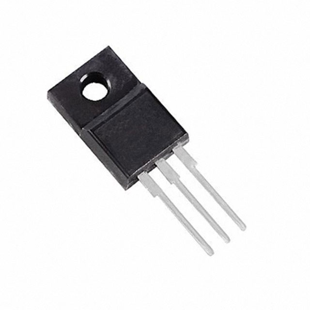
STF18N60DM2

Why Choose Us?
Professional Platform
B2B & B2C purchasingDelivery at full speed
1-2 days deliveryWide variety
Original manufacturers365 days guarantee
Responsible quality
.png)


Tech Specifications
STF18N60DM2 Description
STF18N60DM2 Description
The STF18N60DM2 is a high-performance N-Channel MOSFET from STMicroelectronics, designed for a wide range of applications requiring high voltage and current capabilities. This device features a robust 600V drain-to-source voltage rating and can handle continuous drain currents up to 13A at 25°C. With a maximum power dissipation of 25W, the STF18N60DM2 is well-suited for demanding power electronic applications.
STF18N60DM2 Features
- 600V Drain-to-Source Voltage (Vdss): Ensures reliable operation in high-voltage environments.
- 13A Continuous Drain Current (Id) @ 25°C: Provides ample current handling capabilities for various power electronic applications.
- 25W Maximum Power Dissipation (Tc): Allows for efficient heat management in demanding conditions.
- Low Rds On (Max) @ Id, Vgs: 295mOhm @ 6A, 10V, contributing to high efficiency and low power loss.
- 5V Vgs(th) (Max) @ Id: Facilitates easy gate drive and control.
- Through Hole Mounting Type: Offers flexibility in PCB design and ease of integration.
- TO220FP Package: Provides a compact and robust package suitable for various applications.
- REACH Unaffected and RoHS3 Compliant: Ensures environmental compliance and sustainability.
- Moisture Sensitivity Level (MSL) 1: Allows for unlimited storage time, reducing handling concerns.
STF18N60DM2 Applications
The STF18N60DM2 is ideal for applications that require high voltage and current handling capabilities, such as:
- Power Supplies: Utilized in switching power supplies for efficient voltage regulation.
- Motor Controls: Employed in motor drive circuits for precise speed and torque control.
- Industrial Automation: Used in control systems for reliable and robust operation in harsh environments.
- Automotive Applications: Suitable for in-vehicle power electronics, such as battery management systems and electric power steering.
Conclusion of STF18N60DM2
The STF18N60DM2 from STMicroelectronics stands out as a versatile and robust MOSFET, offering a combination of high voltage, current, and power capabilities. Its low Rds On and easy gate drive make it an excellent choice for high-efficiency power electronic designs. With its compliance to environmental standards and moisture sensitivity level, the STF18N60DM2 is not only a high-performing device but also an environmentally conscious option for various applications in power electronics and industrial control systems.
FAQ
| Quantity | Unit Price | Ext. Price |
|---|---|---|
| 1+ | $3.35828 | $3.36 |
| 10+ | $2.85943 | $28.59 |
| 50+ | $2.56457 | $128.23 |
Not available to buy online? Want the lower wholesale price? Please Send RFQ to get best price, we will respond immediately


.png?x-oss-process=image/format,webp/resize,h_32)


