
STMicroelectronics
STP80NF10
Single FETs, MOSFETs


.png?x-oss-process=image/format,webp/resize,p_30)


STP80NF10 Description
STP80NF10 Description
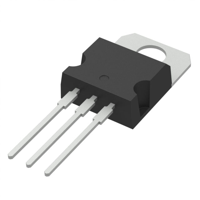
The STP80NF10 from STMicroelectronics is an N-channel 100V, 80A power MOSFET housed in a TO-220AB package, designed for high-efficiency power switching applications. Part of the STripFET™ II series, it leverages advanced Metal Oxide Semiconductor (MOSFET) technology to deliver low on-resistance (15mΩ @ 40A, 10V) and high power dissipation (300W (Tc). With a gate charge (Qg) of 182nC @ 10V and an input capacitance (Ciss) of 5500pF @ 25V, it ensures fast switching performance while minimizing conduction losses. The device is RoHS3 compliant, REACH unaffected, and rated for MSL 1 (Unlimited) moisture sensitivity, making it suitable for industrial and automotive environments.
STP80NF10 Features
- Low Rds(On): 15mΩ (max) at 40A, 10V, reducing conduction losses.
- High Current Handling: 80A continuous drain current (@ 25°C) for robust power delivery.
- Fast Switching: Optimized gate charge (182nC @ 10V) and capacitance for efficient high-frequency operation.
- Thermal Performance: 300W max power dissipation (Tc) ensures reliability under heavy loads.
- Wide Vgs Range: ±20V gate-to-source voltage tolerance for flexible drive compatibility.
- Durability: TO-220AB package offers mechanical strength and heat dissipation.
- Compliance: ROHS3, REACH, and EAR99 certified for global use.
STP80NF10 Applications
- Power Supplies: High-efficiency DC-DC converters, SMPS, and voltage regulators.
- Motor Control: Ideal for H-bridge and brushless DC (BLDC) motor drives.
- Automotive Systems: Used in ECUs, LED drivers, and battery management.
- Industrial Equipment: Inverters, UPS systems, and solenoid drivers.
- Energy Management: Solar inverters and power distribution systems.
Conclusion of STP80NF10
The STP80NF10 stands out for its low Rds(On), high current capability, and thermal efficiency, making it a top choice for demanding power electronics. Its STripFET™ II technology ensures superior switching performance, while the TO-220AB package provides ruggedness for harsh environments. Whether in industrial automation, automotive, or renewable energy, this MOSFET delivers reliability and performance, backed by STMicroelectronics' quality assurance.
Tech Specifications
STP80NF10 Documents
Download datasheets and manufacturer documentation for STP80NF10
 TO-220 ECOPACK 2 graded moulding compound assembly capacity expansion - Subcontractor PSI Laguna (Philippines) (PDF) Product / Process Change Notification (PDF) Product Change Notification (PDF) PRODUCT CHANGE NOTIFICATION (PDF)
 Shopping Guide


.png?x-oss-process=image/format,webp/resize,h_32)


