
STMicroelectronics
STP10N95K5
Single FETs, MOSFETs


.png?x-oss-process=image/format,webp/resize,p_30)


STP10N95K5 Description
STP10N95K5 Description
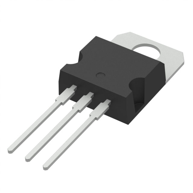
The STP10N95K5 is a high-performance MOSFET (Metal Oxide) from STMicroelectronics, designed for applications requiring robust power handling and high voltage tolerance. With a drain-to-source voltage (Vdss) of 950V and a continuous drain current (Id) of 8A at 25°C, this N-channel device is well-suited for demanding power electronics applications. Its low on-resistance (Rds On) of 800mOhm at 4A and 10V, along with a maximum gate-source voltage (Vgs) of ±30V, ensures efficient operation and control. The STP10N95K5 is mounted through-hole and packaged in a tube, making it easy to integrate into various designs.
STP10N95K5 Features
- High Voltage Tolerance: The STP10N95K5 can handle a drain-to-source voltage of up to 950V, making it ideal for high-voltage applications.
- Low On-Resistance: With an Rds On of just 800mOhm at 4A and 10V, this MOSFET offers low power dissipation and high efficiency.
- Robust Current Handling: Capable of handling a continuous drain current of 8A at 25°C, the STP10N95K5 is suitable for applications requiring high current.
- Wide Gate Voltage Range: The maximum gate-source voltage of ±30V allows for flexible control of the device.
- Low Gate Charge: A maximum gate charge (Qg) of 22nC at 10V contributes to the device's high-speed switching capabilities.
- High Power Dissipation: The STP10N95K5 can dissipate up to 130W, making it suitable for power-intensive applications.
- Compliance: This device is REACH unaffected, RoHS3 compliant, and classified under ECCN EAR99, ensuring regulatory compliance for various markets.
STP10N95K5 Applications
The STP10N95K5 is ideal for a variety of high-voltage and high-current applications, including:
- Power Supplies: Its high voltage and current ratings make it suitable for power supply designs.
- Motor Controls: The device's robust performance is well-suited for motor control applications, where high voltage and current handling are required.
- Industrial Automation: The STP10N95K5 can be used in industrial automation systems that demand high reliability and performance.
- Automotive Electronics: This MOSFET is suitable for automotive applications, such as electric vehicle charging systems and power management.
Conclusion of STP10N95K5
The STP10N95K5 from STMicroelectronics is a powerful MOSFET designed for high-voltage and high-current applications. Its unique combination of high voltage tolerance, low on-resistance, and robust current handling make it an excellent choice for power electronics, motor controls, industrial automation, and automotive electronics. With its compliance with various regulations and its high power dissipation capabilities, the STP10N95K5 is a reliable and efficient solution for demanding applications.
Tech Specifications
STP10N95K5 Documents
Download datasheets and manufacturer documentation for STP10N95K5
 IPD/15/9124 20/Mar/2015
  ST(B,F,P,W)10N95K5
  ST(B,F,P,W)10N95K5
 Shopping Guide


.png?x-oss-process=image/format,webp/resize,h_32)


