
 German
 Japanese
 Portuguese
 Korea
Korea
 Mexico
 Dutch
Dutch


Gate Driver IC Guide: Circuit Topologies, High-Side & Isolated Drivers, Transformer Drive, MOSFET/IGBT Design, Boards & Fault Fixes

Gate driver IC
A gate driver IC is an integrated circuit that converts logic-level control into high-current, fast edges to switch MOSFETs/IGBTs safely and efficiently. Use a gate driver IC whenever switching speed, voltage, isolation, or protection requirements exceed what a bare MCU/FPGA pin can provide.
- Switching frequency ≥ 20–50 kHz → MCU pin rise/fall too slow, switching loss increases.
- Gate charge Qg ≥ 20–50 nC or required peak gate current ≥ 0.5–2 A.
- Topologies with high-side / half-bridge / full-bridge / three-phase devices.
- Need isolation/CMTI robustness (harsh dv/dt, SiC/GaN/IGBT) or safety insulation.
- Need protections: UVLO, DESAT/soft turn-off, Miller clamp, dead-time, diagnostics.

| Topology | Bootstrap? | Isolation typical | Typical bus | Notes |
|---|---|---|---|---|
| Low-side | No | Optional | 12–100 V | Simplest; good for synchronous rectifiers. |
| High-side | Yes (common) | Often needed | 24–600 V+ | Bootstrap limits 100% duty; see high-side. |
| Half-bridge | Yes (HS) | Common | 48–800 V | Dead-time & delay matching are critical. |
| Full-bridge | Yes (2×HS) | Common | 48–800 V | Skew/propagation mismatch can cause shoot-through. |
| Three-phase | Yes (3×HS) | Common | 200–800 V | Use matched multi-channel or isolated drivers. |
Isolation essentials
- Non-isolated vs isolated (magnetic/capacitive/optical) depends on safety and noise immunity.
- CMTI requirement rises with SiC/GaN/fast IGBT; select drivers with high dv/dt tolerance.
- When primary/secondary grounds must be broken or 100% duty is needed, consider a gate driver transformer.
Smart protections to look for
- UVLO on input/driver rails for clean turn-on/off thresholds.
- DESAT + soft turn-off (fast short-circuit protection; vital for IGBT/SiC).
- Miller clamp, programmable dead-time, cross-conduction prevention.
- Diagnostics: FAULT, EN, optional SPI telemetry.
Pdrive ≈ Qg · Vg · f
Example: Qg=80 nC, Vg=10 V, f=100 kHz → Pdrive≈0.08 W. (Rule of thumb: Ipeak ≈ Qg/tr.)
Common pitfalls
- Driving directly from MCU → slow edges, excess switching loss & heating.
- Bootstrap high-side assumed 100% duty → see limitations.
- Poor ground/reference routing → false triggering or damage; see layout tips.
What is a gate driver IC?
Do I need a gate driver?
Gate Driver Circuit
A gate driver circuit combines the driver IC, its supply (or bootstrap/isolated power), and the gate network (Rg/Miller clamp/snubber) with a tight return path. Start by choosing the topology—low-side, high-side, half-bridge, or full-bridge—then solve supply and timing (dead-time & propagation delay matching).
.png?x-oss-process=image/auto-orient,1/quality,q_70/format,webp)
| Topology | Driver form | Supply method | Timing essentials | Common pitfalls |
|---|---|---|---|---|
| Low-side | Single-channel non-isolated | Local 10–15 V rail | Minimal skew; set Rg for EMI vs speed | Long gate loop; Miller turn-on; poor return path |
| High-side | High-side channel (often with LS) | Bootstrap or isolated supply | Duty-cycle windows for Cboot recharge | Assuming 100% duty; insufficient Cboot; dv/dt false turn-on |
| Half-bridge | Dual (HS+LS) matched channels | Bootstrap HS + local LS or isolated dual | Dead-time & delay matching between arms | Shoot-through from skew; cross-coupled ringing |
| Full-bridge | Two half-bridges (4 channels) | As above ×2; often isolated | Cross-leg sync; diagonal conduction prevention | Mismatch between legs; dead-time too short/long |
Supply & bootstrap (quick rules)
- Bootstrap needs low-side on-time to recharge. For sustained high duty or very low frequency, switch to an isolated gate driver or isolated supply.
- Size the capacitor: Cboot ≥ (Qtotal + Qleak + margin) / ΔVallow, where Qtotal includes high-side Qg and driver overhead.
- Place diode, Cboot, and return as a compact loop close to the driver pins.

Dead-time & propagation delay matching
- Too short → shoot-through; too long → body-diode conduction & loss.
- Prefer drivers with matched channels and adjustable dead-time; verify skew over temperature.
- Measure at gate-to-emitter/source (Kelvin) with a differential probe.

Gate network basics
- Use split Rg (pull-up/pull-down) to balance EMI vs switching loss.
- Miller clamp or small negative bias helps against dv/dt induced turn-on.
- RC snubber/damping to control ringing; minimize gate loop area; prefer Kelvin source packages.

high side gate driver (bootstrap duty-cycle limits)
A high side gate driver often relies on a bootstrap diode and capacitor. At very high duty cycles, low frequency, or light load, recharge windows shrink and the high-side supply sags. Options: shorten the max duty window, add assisted charge (charge pump/aux path), or move to an isolated driver/supply. See more in High-side gate driver.

difference between half bridge and full bridge gate driver
- Channels & packaging: half-bridge = HS+LS pair (1 IC or two singles); full-bridge = two half-bridges (4 channels).
- Timing complexity: full-bridge needs cross-leg synchronization and diagonal conduction prevention; skew compounds across legs.
- Thermal & drift: tighter channel-to-channel matching and temperature stability are preferred in full-bridges.

- Shortest gate/return loop; keep driver ground referenced tightly to the power device (Kelvin source).
- Local decoupling near driver pins (small ceramic + bulk).
- Separate signal and power routing; avoid long parallel runs between gate traces and power loops.
- Plan FAULT/UVLO/EN pull resistors and power-up sequence.
- Probe VGS/GE locally with a differential probe for truthful timing.
What is a gate driver circuit?
Why do dead-time and delay matching matter?
High Side Gate Driver
A high side gate driver floats on the switch node (HS) and commonly uses a bootstrap diode + capacitor to power the high-side channel. Bootstrap cannot sustain true 100% duty and is sensitive to dv/dt and power-up transients. If duty-cycle or common-mode noise exceeds the bootstrap window, switch to an isolated gate driver.

Bootstrap operation & limits
- Low-side ON creates a recharge window through the diode; high-side ON consumes charge from CBOOT.
- Very high duty, very low frequency, or light load → recharge windows shrink → VHB droops → UVLO trips or HS gate collapses.
- Place the diode, CBOOT, and driver pins in a tight loop; use fast/Schottky diode and X7R capacitor with derating margin.
CBOOT ≥ (Qtotal + Qleak + margin) / ΔVallow
Rule of thumb: start with CBOOT ≈ 10–20 × Qg(HS), then verify leakage & duty-cycle. Use ΔVallow=0.2–0.5 V.
Reaching near-100% duty
- Duty management: inject short refresh pulses (simple but may not fit tight control specs).
- Assisted charge: charge-pump/aux recharge path (limited current and frequency range).
- Upgrade path: move to an isolated gate driver/supply for true 100% duty and long static ON time (recommended).
dv/dt robustness & Miller false turn-on
- Switch-node dv/dt injects IMiller ≈ Cgd·(dv/dt) into the gate → false turn-on risk.
- Mitigation: Miller clamp, modest negative gate bias, split Rg (faster pull-down), and RC damping/snubber.
- Minimize gate/return loop; prefer Kelvin source; select drivers with high CMTI ratings.
Power-up transients & UVLO
- Bus ramp and undefined nodes can spur unintended turn-on. Keep the gate hard-pulled down until UVLO thresholds are met.
- Sequence EN/FAULT lines; verify thresholds and blanking; measure local VGS/GE with a differential probe (not at the controller).
- Compact triangle loop: driver pin → diode → CBOOT → back to driver.
- Local decoupling (small ceramic + bulk) right at the driver pins.
- Short, direct gate and return; keep away from high-current power loops.
- Verify dead-time & propagation skew across temperature; stress-test high dv/dt.
- For sustained high duty or static ON, prefer isolated high-side.
Why can’t bootstrap reach true 100% duty?
How to stop high-side false turn-on with fast dv/dt?
Isolated Date Driver
An isolated gate driver provides signal and/or power isolation with high CMTI, ideal for high-voltage nodes, harsh dv/dt, multi-ground systems, and true 100% duty operation. When bootstrap can’t meet duty-cycle or noise immunity, migrate to an isolated gate driver.

Why isolated gate driver?
- Safety/insulation: meet basic/functional/reinforced insulation needs for human and system safety.
- Noise/CMTI: withstand fast switch-node dv/dt (SiC/GaN/IGBT) to avoid false turn-on.
- System architecture: break ground loops in multi-module or long-cable designs; support distributed gate power.
- Definition: Common-Mode Transient Immunity (kV/µs) — immunity to rapid common-mode voltage steps.
- Targets (rule of thumb): mainstream MOSFET/IGBT ≥ ~50 kV/µs; SiC/GaN scenarios aim ≥ ~100 kV/µs.
- Datasheet reading: rely on minimum spec and test conditions; combine with Miller clamp / negative bias if needed.
Isolation levels (basic / functional / reinforced)
- Basic: single insulation for basic protection.
- Functional: ensures operation but not necessarily human safety.
- Reinforced: single barrier with protection equivalent to double insulation.
Engineer’s checklist: isolation voltage rating, creepage/clearance, lifetime curves, surge/partial-discharge margins versus your target standard.
Two paths to isolation
- Isolated gate driver IC: integrated digital isolation; add isolated DC-DC if gate power is needed. Compact and feature-rich.
- Gate driver transformer: robust for extreme CMTI/temperature and symmetric drive; requires reset strategy and waveform conditioning.
difference between IGBT and MOSFET gate driver
- VDRV: MOSFET commonly +6~10~12 V; IGBT typically +15 V to ensure conduction and minimize loss.
- Negative gate bias: MOSFET often 0 V off; high-speed/SiC/GaN may use −2~−3 V. IGBT often uses about −5 V for robust turn-off.
- DESAT & soft turn-off: critical for IGBT/SiC short-circuit survival; MOSFET can use other OCP schemes but DESAT is common on IGBT/SiC drivers.
Migrating from MOSFET to IGBT/SiC? Upgrade driver capability: higher VDRV, negative bias, DESAT/CMTI, and matched timing.
- Keep primary/secondary loops tight and locally closed; minimize loop areas on both sides of the barrier.
- Place isolated power and driver decoupling right at pins.
- Short, paired gate/return routing; prefer Kelvin source/emitter packages.
- Probe local VGS/GE with a differential probe to avoid common-mode artifacts.
- Provide FAULT/EN lines and a defined soft turn-off path.
Why choose an isolated gate driver over bootstrap?
How much CMTI do I need?
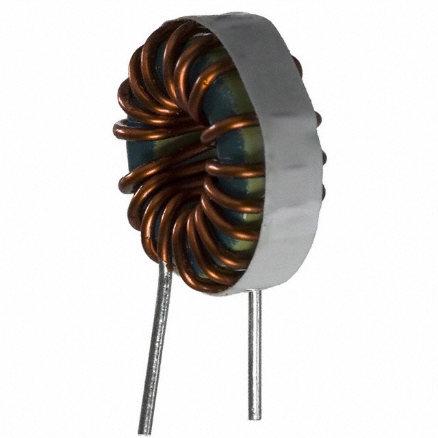
Gate Driver Transformer / Transformer Gate Drive
A gate driver transformer (GDT) transfers isolated gate energy via magnetic coupling with extremely high CMTI and harsh EMC tolerance. It excels in symmetric drive and wide temperature ranges, but demands proper reset (demagnetization) and good symmetry—otherwise droop and false turn-on can occur. If you need true 100% duty or long static ON time, consider an isolated gate driver.

Why use a gate drive transformer?
- Extreme CMTI and isolation robustness across long distances and noisy power stages.
- Wide temperature / high power suitability versus some capacitive/digital isolation schemes.
- System partitioning: break ground loops; support distributed gate power islands.
Need continuous 100% duty or long static ON? Prefer an isolated gate driver with isolated power.
How does a transformer gate drive work?
- Flux balance: each primary pulse pushes ΔB; a proper reset path must pull flux back (−ΔB) before the next pulse to avoid core saturation.
- Reset strategies: bipolar push-pull (natural reset), dedicated reset winding/diode, or series DC-blocking capacitor + bleed for zero-DC balance.
- Wave shaping: secondary clamps (diode/Zener), split Rg, and strong pull-down (or negative bias) to get clean +VG/0 or +/− gate waveforms.
- Drive power: Pdrive ≈ Qg · Vg · f — same entry point as IC drivers.
- Turns / core window (avoid saturation): N ≥ V · tpulse / (ΔBallow · Ae). Choose ΔBallow per material; derate for temperature.
- Turns ratio: set Np:Ns for target VG,ON after losses; verify clamping and shaping margins.
- Leakage inductance: interleave/layer windings for tight coupling to speed edges and reduce ringing.
- Frequency window: very low f or prolonged duty → reset risk; very high f → leakage and core loss dominate.
Common issues & risks
- Insufficient demagnetization → flux walk & saturation → waveform collapse or unintended turn-off.
- Poor symmetry → DC bias at the gate → false turn-on or gate overstress.
- High leakage → slow edges and heavy ringing; fix layout/winding scheme and add damping.
- Weak secondary shaping → turn-off tails/overshoot; add strong pull-down, clamp, or negative bias.
How to make a gate drive transformer (steps)
- Collect specs: VG,ON/VG,OFF, Qg, f, allowable droop, ΔBallow, isolation/CMTI.
- Select core/material by frequency & temperature; get Ae and window factor.
- Estimate turns: N ≥ V · tpulse / (ΔBallow · Ae); refine for droop/leakage.
- Plan coupling: interleave/layer; optional shield with awareness of parasitic capacitance.
- Secondary shaping: clamp (diode/Zener), split Rg, and optional negative bias; verify rise/fall and overshoot.
- Reset strategy: bipolar drive/reset winding/series DC-block; measure flux reset each cycle.
- Validate: hot-soak dv/dt, duty edges, long ON tests, short/open gate fault tolerance.
Why choose a gate drive transformer over an isolated driver IC?
How do I avoid saturation and waveform droop?
Gate Driver for MOSFET
A gate driver for MOSFET (or gate driver circuit for MOSFET) pairs a driver IC with a tuned gate network (split Rg/Miller clamp/snubber) and a tight return path. The goal is to balance EMI and loss: decide target dv/dt / tr, tf, then back-solve Rg and drive current.

Ipeak ≈ Cg · (dv/dt)
Rg_init ≈ (tr · Vgate) / Ipeak
Then verify driver source/sink current ≥ Ipeak and check drive loss Pdrive=Qg·Vg·f (see gate driver design).
MOSFET gate network in 6 steps
- Collect Qg, Ciss/Crss(≈Cgd), Vth, VGS ratings, RDS(on)-vs-VGS.
- Set target edges tr/tf or dv/dt (trade EMI vs efficiency/diode recovery).
- Estimate Ipeak (≈ Cg·dv/dt, or ≈ Qg/tr as a shortcut).
- Compute Rg_init ≈ (tr·Vgate)/Ipeak; start with E12/E24 ladder values.
- Use split Rg (up/down): smaller pull-down to strengthen turn-off & Miller immunity; add diode+resistor to shape asymmetry if needed.
- Verify driver current and thermal headroom; iterate with bench data (scope local VGS).
Ringing: diagnosis & mitigation
- Minimize loop: keep driver–gate–source (Kelvin source) loop short; avoid parallel runs with power loops.
- Shape the network: split Rg, add RC damper or small ferrite bead; consider a gate clamp (diode/Zener) for overshoot.
- Measure right: differential probe at the device pins; watch Miller plateau and overshoot.
Miller clamp & negative gate bias
- Miller clamp: prioritize for high dv/dt, large Cgd, paralleled devices, or long gate wiring to prevent false turn-on.
- Negative bias (≈ −2~−3 V): consider for fast MOSFET/SiC or harsh dv/dt; ensure VGS(min) margins and driver ratings.
- Typical path: start with clamp, then evaluate small negative bias; both can coexist.
- Split Rg,up / Rg,down; diode bypass to realize fast-off/slow-on or vice versa.
- Optional Cgs/RC damper for high-frequency ringing control.
- Gate clamp (Zener/TVS) for transient over-voltage; check leakage and dynamic thresholds.
- Shortest Kelvin return and local decoupling at the driver pins.
when to use a gate resistor
Use a gate resistor when edges are too fast (EMI), diode recovery spikes are severe, devices are paralleled, or gate wiring is long/parasitics are high. Reduce Rg when the layout is tight, Qg is small, and bus voltage is low. Start from Rg_init and A/B test a few ladder values.
how to select gate resistor for MOSFET
Follow the 6-step flow above: set dv/dt targets, compute Ipeak & Rg_init, split pull-up/down, match paralleled gates, and iterate on bench with thermal/EMI observations. Prefer stronger pull-down for Miller immunity.
- Shortest driver–gate–source path; Kelvin source; local decoupling.
- Pair gate and return traces; limit vias/series inductance.
- Verify tr/tf/dv/dt and VGS overshoot hot/cold; observe the Miller plateau.
- Match channels in paralleled devices (Rg, routing symmetry).
- Escalate tricky waveforms to gate driver fault troubleshooting.
IGBT Gate Driver
An IGBT gate driver typically uses +15 V turn-on, a modest negative gate bias for turn-off (≈ −5 V), and DESAT detection with soft turn-off to survive short circuits. Provide a reverse (freewheel) diode for current commutation. For high dv/dt/high-voltage stages, prefer an isolated gate driver.

Drive bias & gate control
- VDRV: use about +15 V to reduce conduction loss and ensure strong saturation.
- Negative gate bias: ≈ −5 V improves dv/dt immunity and reduces false turn-on; combine with a Miller clamp.
- Split Rg: stronger pull-down than pull-up; match channels across paralleled devices.
- Layout: Kelvin emitter return, shortest gate/return loop, local decoupling right at the driver pins.
- Principle: sense VCE via DESAT path; if it exceeds a threshold above normal VCE(sat), declare a short/hard saturation.
- Timing: blanking after turn-on → DESAT threshold trip → soft turn-off to limit dI/dt and over-voltage → fault report/latch.
- Engineering knobs: choose threshold with margin over load VCE(sat); set soft-off slope to avoid over-voltage/thermal stress.
- Route DESAT diode/sense lines short and away from high dv/dt nodes; verify behavior hot/cold.
Reverse current path (freewheel diode)
- An IGBT needs a reverse diode for current commutation; select by surge capability, recovery Qrr, and thermal limits.
- Modules may integrate the diode; in discretes, co-design diode and snubbers to manage recovery stress.
- Compare to MOSFET: body diode is inherent in MOSFETs, but recovery/EMI still need attention.
- SC withstand time is typically microseconds-class → DESAT + fast soft-off are mandatory.
- Over-voltage control: RC/TVS/active clamp to limit turn-off overshoot.
- Fault policy: latch & cooldown before retry; log FAULT status.
- Measure local VGE and VCE with differential probes; record dI/dt and VCE peaks.
- Kelvin emitter reference; short, paired gate/return routing.
- Shortest DESAT paths; keep away from switch-node dv/dt fields.
- Decouple driver rails at pins (small ceramic + bulk).
- Plan FAULT/EN pull resistors and power-up order.
- Validate soft-off slope, overshoot clamps, and channel matching over temperature.
is MOSFET better than IGBT
It depends on bus voltage and frequency: low-voltage (≤200–300 V) and high-frequency favor MOSFETs; mid/high voltage (≥600–1200 V) and large currents often favor IGBTs. IGBTs need +15/−5 V, DESAT, and soft-off; MOSFETs emphasize RDS(on) and gate-charge trade-offs.
can IGBT replace MOSFET
Not pin-to-pin. You must re-evaluate frequency/efficiency targets, add a reverse diode, change drive bias (+15/−5 V), and implement DESAT/soft-off. At low voltage/high frequency, MOSFETs are usually preferable.
why is IGBT used in VFD
Typical VFD buses run ~600–1200 V with moderate switching frequencies and high currents. IGBT modules offer robust conduction, short-circuit survivability (with proper protection), thermal handling, and cost advantages.
why is thyristor not used in an inverter
Thyristors require commutation and have slow turn-off, making high-frequency PWM in modern inverters impractical. IGBT/MOSFET devices suit PWM control; GTO/IGCT are special cases with higher complexity.
Gate Driver Design
Practical gate driver design = timing match (propagation & dead-time) + noise immunity (CMTI, layout) + stable supplies (decoupling/return path) + protections (UVLO/DESAT/soft-off). Decide topology & isolation first, shape the gate network next, then lock layout and measurement.

End-to-end design flow (8 steps)
- Inputs: VBUS, device (MOSFET/IGBT/SiC), Qg/Crss, f, efficiency/EMI targets, safety.
- Topology & isolation: low/high-side, half/full-bridge, 3-phase; bootstrap vs isolated or GDT.
- Driver selection: peak source/sink, CMTI, UVLO, DESAT/soft-off, Miller clamp, channel matching.
- Gate network: split Rg, RC damper/ferrite, gate clamp, optional negative bias (see MOSFET section).
- Timing: set dead-time; verify tPLH/tPHL and channel/temperature mismatch (Δt).
- Supply & decoupling: bootstrap sizing or isolated DC-DC; local X7R ceramics + bulk; minimize supply loops.
- Protections: UVLO thresholds, DESAT with soft-off ramp, turn-off over-voltage clamps (RC/TVS/active).
- Layout & validation: Kelvin source/emitter, tight gate/return loop, differential VGS/GE probing; hot/cold & high dv/dt stress; escalate oddities to fault.
- Propagation mismatch: use drivers with tight channel-to-channel skew; target Δt in the few-tens-of-ns class.
- Dead-time lower bound: ≥ (max mismatch + diode reverse-recovery window). Too short → shoot-through; too long → diode loss.
- Measure at the device: probe local VGS/VGE (Kelvin) across temperature; not at the controller pins.
CMTI & isolation choices
- Mainstream MOSFET/IGBT aim for ≥ ~50 kV/µs CMTI; SiC/GaN often ≥ ~100 kV/µs.
- Harsh dv/dt or multi-ground systems → prefer isolated gate driver or GDT plus Miller clamp/negative bias.
Decoupling & return path (layout)
- Place driver decoupling right at pins (multiple small ceramics in parallel + a local bulk cap).
- Bootstrap diode and CBOOT in a compact triangle loop; see high side.
- Route gate and return as a paired, short path; avoid long parallel runs with power loops.
what is gate driving loss of MOSFET
Average driver power per channel arises from charging/discharging the gate: Pdrive = Qg · Vg · f. It scales linearly with frequency, gate voltage, and total gate charge, largely independent of load power.
- Thermal budget: sum across channels and add driver self-loss; check package θ and copper spreading.
- Mitigation: lower Qg/Vg or split channels; ensure driver peak current meets Ipeak while staying cool.
- See MOSFET gate network for Ipeak/Rg setup.
How do I set dead-time?
Gate Driver Board
A gate driver board (EVB/prototype) combines the driver IC, isolation/supply, and a tuned gate network on a layout that respects test points, creepage/clearance, ground partitioning, and measurement best practices. Good probing and return-path planning decide whether bring-up is smooth and data is trustworthy.

Board structure & partition
- Power / Driver / Control zones separated; slot or keep clearance between HV and LV domains.
- Shortest driver–gate–Kelvin source/emitter loop; place return via next to the gate via.
- Bootstrap triangle loop (driver pin–diode–CBOOT) or isolated DC-DC decoupling at pins.
- Local VGS/GE (Kelvin), VBOOT/VHB, driver rails (VDD, VEE), FAULT/EN.
- DESAT node (IGBT/SiC), HS switch node (observe dv/dt alongside gate).
- Optional: current shunt/Hall/Rogowski header, thermocouple pads, logic debug header.
Ground planning & return paths
- Small-signal driver ground ties to power return via single-point or narrow bridge.
- Route gate and return as a paired short path; avoid long parallel runs near power loops.
- Keep isolation domains locally closed; do not stitch grounds across the barrier.
- Mark HV/LV boundary on silkscreen; reserve no-copper keepouts and avoid vias across the isolation moat.
- Size distances per your standard and bus voltage; consider altitude and pollution degree; use slots to boost creepage.
- Respect isolation component ratings (basic/functional/reinforced) and follow their layout notes.
- Do use differential probes / coax short ground; Don’t use long alligator ground leads.
- Do probe local device pins (Kelvin) for VGS/GE; Don’t probe at the controller.
- Do bandwidth-limit to see the true shape; Don’t misread probe resonances as ringing.
- Do observe HS node with VHB droop; Don’t look at gate alone on high-side debugging.
- Static checks: UVLO rails, polarity, isolation direction, CBOOT/diode orientation.
- Low-voltage smoke test: reduced rails, no load; verify FAULT/EN, propagation delay.
- Single-leg / low duty: ramp frequency/duty; watch VGS plateau, VHB droop.
- Full-bridge / 3-phase: validate dead-time and inter-leg skew.
- Corner cases: hot dv/dt, load steps; record fault behavior and overshoot clamps.
Configurability & safety hooks
- Jumpers/DIP: split Rg steps, negative bias on/off, Miller clamp enable, soft-off slope options.
- Protection tuning: accessible DESAT threshold/blanking cap; pads for RC/TVS/active clamp.
- Safety: HV markings, low-voltage guard area, discharge resistors, interlock header.
BOM notes
- Rg ladder (E24/E96), CBOOT X7R with voltage derating; fast/Schottky diodes.
- Drivers with matched channels and high CMTI; isolated DC-DC with pulse-current headroom.
How do I probe VGS without adding ringing?
How much clearance/creepage should I keep?
Gate Driver Fault
Typical gate driver faults come from floating gates, ringing & false turn-on, dead-time/skew issues, DESAT trips, insufficient CMTI, and bootstrap sag. Start with correct probing (local differential VGS/GE + HS node), then use the symptom → cause → action checklist below.

| Symptom | Likely causes | Immediate actions | See also |
|---|---|---|---|
| Random turn-on / unstable OFF | Floating gate; weak pull-down; dv/dt-induced Miller injection | Add pull-down; split Rg with stronger down; Miller clamp / slight negative bias | floating gate · MOSFET gate network |
| Strong ringing / overshoot | Large loop inductance; poor routing; excessive edge speed; snubber missing | Shorten gate/return loop; split Rg; RC damper or ferrite; gate clamp | ringing in MOSFET · design rules |
| Shoot-through / cross-conduction | Dead-time too short; propagation skew; Miller false turn-on of the opposite device | Increase dead-time; match channels; add clamp/negative bias; verify at device pins | timing & dead-time |
| DESAT trip / short-circuit events (IGBT/SiC) | Real SC; threshold too low; blanking too short; noisy sense wiring | Tune threshold/blanking; route DESAT short; verify soft turn-off & clamps | IGBT gate driver |
| High-side drops out at high duty/low f | Bootstrap can’t recharge; VHB droop; UVLO hit | Assisted recharge; reduce duty; switch to isolated driver | high side · isolated |
what happens if a MOSFET gate is floating
A floating gate picks up noise and may randomly turn on, causing heat and EMI. Provide a defined OFF path: add a gate pull-down (≈47–220 kΩ), use stronger pull-down than pull-up, and consider a Miller clamp or small negative bias. See MOSFET gate network and layout rules.
what is ringing in MOSFET
Parasitic Lloop with device capacitances (Coss, Cgs) forms a resonant tank → visible overshoot/undershoot. Fix with a short paired gate/return loop (Kelvin), split Rg, RC damper or ferrite bead, and an appropriate gate clamp. Probe with a differential head at the pins and bandwidth-limit to avoid “fake ringing.”
why does MOSFET damage / what kills a MOSFET
Usual killers: VGS over-voltage, VDS overshoot/avalanche, SOA violation, dv/dt-induced false turn-on leading to shoot-through, thermal runaway, or oscillation. Increase dead-time and channel matching, strengthen pull-down, enable Miller clamp or light negative bias, add over-voltage clamps/snubbers, and optimize layout. See design.
can IGBT block reverse voltage
Standard IGBTs do not reliably block reverse voltage. You typically need a freewheel diode for reverse current. Special RB-IGBTs exist but are uncommon. See IGBT gate driver.
- Reproduce safely: start at reduced rails, single-leg, low duty.
- Probe correctly: local VGS/GE, HS node, VHB/VCE, and current dI/dt with proper sensors.
- Change one variable: Rg, dead-time, topology element; observe trends.
- Identify root cause: if duty/low-f bootstrap sag → switch to isolated driver/fix bootstrap.
- Harden: Miller clamp / negative bias / RC damping / layout rework; consider GDT for extreme CMTI.
- Do use differential probes or coax short-ground kits; Don’t use long alligator grounds.
- Do probe at the device pins (Kelvin); Don’t trust controller-side readings.
- Do view HS node with VHB droop; Don’t look at gate alone on high-side issues.
- Do re-test hot/cold; Don’t rely on room-temp only.
Upload 3 scope screenshots (local VGS/GE, HS node, VHB/VCE or current) plus BOM/driver/topology. We’ll reply with root-cause ranking, 2–3 immediate fixes, and pin-to-pin alternatives.
Submit screenshots via RFQSubmit your BOM (48h)
- Lead-time comparison across brands/channels
- Pin-to-pin alternatives with differences highlighted
- Compliance guidance (AEC-Q / Industrial)
- Sample-kit suggestion for small runs
.png?x-oss-process=image/auto-orient,1/quality,q_70/format,webp)

Related Articles
- ·What Are the Advantages of Micron Technology in Global HBM Memory Competition?
- ·Micron HBM and Advanced Memory: Can It Challenge Samsung and SK Hynix?
- ·AI Demand, HBM Growth, and Memory Market Trends
- ·The Significance of Memory and Storage for AI
- ·Why Memory Capacity Is a Performance Bottleneck for AI Applications
- ·HBM3 vs. HBM3E: Complete Technical Comparison for AI, HPC, and Global Component Procurement
- ·How Large Language Models Work
- ·SK Hynix & Samsung: The Unprecedented HBM Expansion Race
- ·Micron 6600 ION 245TB Redefines Data Center
- ·Why Memory and Storage Define the Next Decade









.png?x-oss-process=image/format,webp/resize,h_32)


