
 German
 Japanese
 Portuguese
 Korea
Korea
 Mexico
 Dutch
Dutch


Schmitt Inverter: Working Principles, Discrete vs IC, Applications & 7-Brand Picks

1) What Is a Schmitt Inverter?
A Schmitt inverter is a NOT gate with input hysteresis (two thresholds UTP / LTP). It converts noisy or slow-ramping inputs into clean digital edges and is widely used for debouncing, edge shaping, and RC oscillators. As a function, it can be implemented with discrete circuitry (comparator/op-amp + positive feedback) or purchased as a standalone IC (e.g., 74HC14 / 74LVC1G14 / CD40106B).
Discrete Path (Comparator / Op-Amp + Positive Feedback)
Customizable thresholds and tight coupling with analog chains; higher tuning effort and part-to-part variance. Mind CMRR, PSRR, quiescent current, and propagation delay.
IC Path (Logic Families with Schmitt Inputs)
Examples: 74HC14 (hex), 74LVC1G14 (single-gate), CD40106B (3–15 V). Consistent thresholds, predictable delay, and simple BOM—great for small footprints and fast time-to-market.
On a rising input, crossing UTP flips the output; on a falling input, going below LTP flips it back. The hysteresis width is UTP − LTP: wider hysteresis increases noise immunity but can add intentional switching latency.
Note: Thresholds depend on supply voltage and logic family (HC/HCT/LVC/4000B). Always check the specific datasheet.
Typical Uses
- Debounce (switch/relay contact de-bounce)
- Slow-ramp cleanup / power-good shaping
- RC oscillator (threshold-based charge/discharge)
- Sensor edge cleaning (thermistor/photodiode/Hall/PLC interface)
“Schmitt” refers to Otto H. Schmitt, who introduced the trigger concept. This page is about logic/signal conditioning devices—not power inverters. Logic shorthand: rising past UTP causes one output transition; falling below LTP causes the opposite transition, creating stable, chatter-free switching.

What does a Schmitt inverter do?
It’s a NOT gate with hysteresis that converts noisy or slow inputs into crisp digital edges—ideal for debounce, edge shaping, and simple RC oscillators.
What is the purpose of a Schmitt trigger?
To provide two distinct thresholds (UTP/LTP) so the output doesn’t chatter at one switching point, improving noise immunity and timing determinism.
What is UTP and LTP?
UTP (upper threshold) is used on rising inputs; LTP (lower threshold) is used on falling inputs. Their difference is the hysteresis width.
What does Schmitt mean?
It’s named after Otto H. Schmitt. In this context, “Schmitt” means an input with hysteresis—nothing to do with power inverters.
Further reading: Comparator Circuit · Submit your BOM
2) Working Principles — Two Paths
2.1 Discrete Path (Comparator / Op-Amp + Positive Feedback)
A Schmitt comparator is built by feeding a portion of the output back to the non-inverting input so the threshold depends on the current state. When the output is high, the feedback lifts the switching point (UTP); when the output is low, it lowers the switching point (LTP). This two-threshold behavior forms hysteresis and eliminates chatter around a single threshold.
Let V+ be formed by a divider between VREF and VOUT via Rref (to VREF) and Rfb (to VOUT). Define β = Rfb / (Rref + Rfb).
UTP: VT+ = VREF + β · (VOH − VREF)
LTP: VT− = VREF + β · (VOL − VREF)
Hysteresis width: ΔVH = VT+ − VT− = β · (VOH − VOL)
Design workflow
- Pick the desired hysteresis width ΔVH from the noise environment (rule of thumb: at least 2–3× peak-to-peak noise).
- Compute β = ΔVH / (VOH − VOL), then choose a convenient ratio for Rfb and Rref.
- Choose VREF to center the thresholds where you need them (e.g., around mid-supply for symmetrical switching).
Example @ 3.3 V: target ΔVH ≈ 0.60 V ⇒ β ≈ 0.60 / 3.3 ≈ 0.182. With Rref=100 kΩ, pick Rfb ≈ (β/(1−β))·Rref ≈ 22 kΩ.
Why a comparator (not a general op-amp)?
- Input structure and recovery optimized for switching; specified propagation delay.
- Open-drain/collector variants allow level shifting and wired-OR.
- Cleaner behavior with large overdrive and near-rail signals.
When an op-amp can be acceptable
- Very low speed and cost sensitive, with input kept within valid common-mode range.
- Saturation is avoided (use clamp/limit) or recovery time is non-critical.
- RRIO op-amps and proper biasing are used for single-supply sensing near ground.
- CMRR: higher CMRR better suppresses common-mode swings on long traces or sensor leads, preventing false trips.
- PSRR: supply ripple shifts thresholds; high PSRR plus decoupling and a filtered reference stabilize VT+/VT−.
- Quiescent current (Iq): sets battery life/thermal headroom; extremely low-Iq devices may have limited speed/drive.
- Speed: check propagation delay vs expected overdrive; don’t make the input network excessively large (≈10–200 kΩ typical).
- Input common-mode violation (especially with op-amps) → use RRIO parts or a true comparator.
- Too little hysteresis → residual chatter; size ΔVH ≥ 2–3× noise p-p.
- Logic-level mismatch at the output → use open-drain + pull-up or add a Schmitt inverter IC.
- Single-supply low-end sensing → add bias to keep inputs in valid range.

How does a Schmitt comparator work?
Positive feedback makes the switching threshold follow the current output: high output raises the threshold (UTP), low output lowers it (LTP). The two thresholds are set by the feedback ratio β and the output swing (see equations above).
What is CMRR / PSRR, and why is higher CMRR better?
CMRR measures rejection of common-mode input changes; higher values prevent false triggers from ground bounce or cable pickup. PSRR measures rejection of supply ripple; it limits threshold drift with noisy rails.
What is the quiescent current?
The supply current with no switching activity. It sets baseline power draw and often trades with speed and output drive capability.
2.2 IC Path (74HC / 74LVC / 4000B Families)
Logic families provide gates with built-in Schmitt inputs, giving consistent thresholds and predictable delays with minimal external parts. Here’s how the common families differ and when to use each.
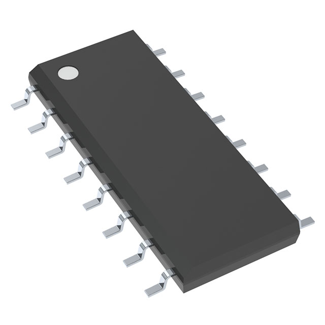
- HC (2–6 V): general CMOS; classic 74HC14 (hex inverting Schmitt) for many 3.3/5 V needs.
- HCT (5 V, TTL thresholds): input thresholds compatible with older TTL logic for mixed systems.
- LVC (1.65–5.5 V): wide supply, fast, often 5 V-tolerant inputs; go-to single-gate: 74LVC1G14; non-inverting buffer: 74LVC1G17.
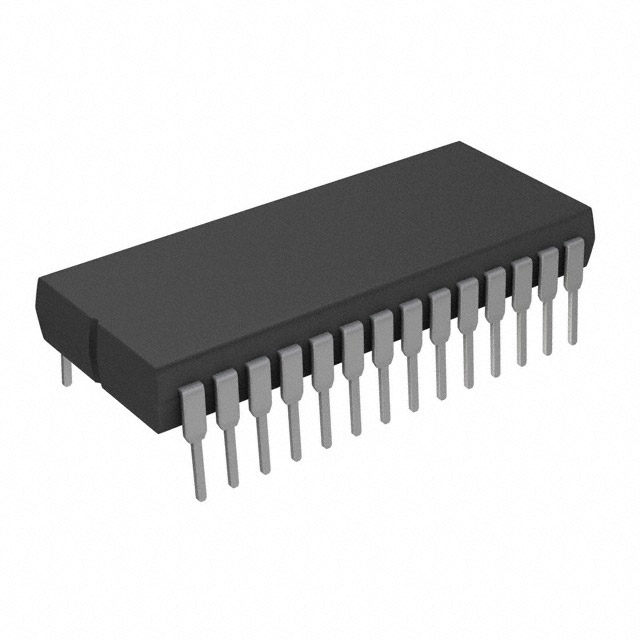
- 4000B (3–15 V): high-voltage, slower, low static power; classic CD40106B (hex inverting Schmitt).
- New 3.3 V / 1.8 V designs: LVC.
- 5 V with TTL compatibility: HCT (or LVC with 5 V-tolerant inputs).
- ≥ 6 V or 12 V domains: 4000B (e.g., CD40106B).
- Many channels / low cost: hex devices (HC14 / 40106B). Local edge clean-up: single-gate 1G14 near the source.

Which IC is used in a Schmitt trigger / for a NOT gate?
For an inverting Schmitt gate: 74HC14, 74LVC1G14, CD40106B. Plain NOT (no hysteresis): 74HC04, 74LVC1G04. Non-inverting Schmitt buffers: 74HC17, 74LVC1G17.
What is a hex Schmitt inverter?
“Hex” means six identical inverting Schmitt gates in one IC (e.g., 74HC14, CD40106B). They’re ideal for multiple switch debouncers, RC oscillators, or channel-by-channel edge cleaning.
Schmitt-trigger buffer vs inverter?
A buffer is non-inverting (e.g., 74LVC1G17); an inverter flips polarity (e.g., 74LVC1G14). Both add hysteresis for noise immunity.
Further reading: Comparator Circuit · RC Oscillator · Submit your BOM
3) Types & Signals
3.1 What counts as a “type”?
- Inverting Schmitt (schmitt trigger inverter) — flips polarity and adds hysteresis. Typical parts: 74HC14, 74LVC1G14, CD40106B.
- Non-inverting Schmitt (schmitt trigger buffer) — preserves polarity while adding hysteresis. Typical parts: 74HC17, 74LVC1G17.
- Integration level — single-gate (1Gxx) for point-of-use edge cleaning vs hex devices for multi-channel debounce/oscillators.
- Output structure — push-pull by default; if you need wired-AND/level shifting, use an open-drain/collector buffer in combination or a comparator with open-drain output.
- Logic family — HC/HCT/LVC/4000B determine supply range, threshold placement, speed, and 5-V tolerance.
3.2 Signals (how the waveforms change)
- Thresholds — rising uses VIH+ (UTP), falling uses VIL− (LTP). Positions depend on family and VCC.
- Hysteresis width — fixed by the IC family (IC path) and tunable in discrete designs; wider hysteresis boosts noise immunity.
- Output drive & delay — check datasheets; LVC is typically faster and can be 5-V tolerant at inputs.
- Effect — slow/noisy analog edges become crisp digital transitions with immunity to small input chatter.
3.3 Non-inverting (two ways to get it)
Dedicated Schmitt buffer
Use a part like 74LVC1G17 / 74HC17. Cleanest option with minimal delay and no polarity flip.
Two inverters in series
Cascade two inverting Schmitt gates (e.g., two 1G14 stages). Pros: widely available; Cons: doubles delay/area.
3.4 Single-gate vs Hex
- Single-gate (1Gxx) — SOT-23/SC-70 footprints; place right at the source for best EMI/edge control.
- Hex — SOIC/TSSOP/DIP with six channels; efficient for many keys, RC oscillators, or multi-line conditioning.
3.5 Push-pull vs Open-drain
- Push-pull — default for Schmitt gates; direct, fast transitions in the same voltage domain.
- Open-drain needs — use a dedicated open-drain buffer (e.g., 1G07/1G06) after the Schmitt stage, or a comparator with open-drain + pull-up for wired-AND or level translation.
- Many channels / low cost: hex inverting (HC14 / CD40106B).
- Point-of-use edge cleanup: 1G14 (inverting) or 1G17 (non-inverting).
- 1.8–5 V modern designs: LVC family.
- 5 V with TTL compatibility: HCT (or LVC with 5-V-tolerant inputs).
- ≥ 6 V / 12 V domains: 4000B (e.g., CD40106B).

How many types of Schmitt triggers are used?
- By polarity: inverting (Schmitt inverter) and non-inverting (Schmitt buffer).
- By integration: single-gate (1Gxx) and hex (six channels per IC).
- By output style: push-pull is typical; open-drain achieved via companion buffers or comparators.
- By family: HC / HCT / LVC / 4000B (different VCC, thresholds, speed, tolerance).
See also: Working Principles — Two Paths · Submit your BOM
4) Discrete vs IC — How to Choose
For most designs, pick a Schmitt inverter IC (e.g., 74LVC1G14 / 74HC14 / CD40106B) for consistent thresholds, small footprint, and fast time-to-market. Choose a discrete schmitt inverter circuit (comparator/op-amp + positive feedback) when you need custom UTP/LTP, unusual supply domains, or tight coupling to analog front-ends. If you build an inverting Schmitt trigger discretely, prefer a comparator over a generic op-amp.
.png?x-oss-process=image/auto-orient,1/quality,q_70/format,webp)
ICs typically win on TTM, threshold consistency, EMI robustness, and board area. Discrete solutions win on threshold programmability, level shifting / wired-AND flexibility, and special supply ranges (e.g., ≥6–15 V or mixed domains). For sheer speed, modern LVC gates are very fast; specialized high-speed comparators can still be preferable when the analog behavior and overdrive profile matter.
BOM & engineering time
IC: one part, minimal tuning. Discrete: resistors/reference/ESD/RC plus validation time.
Threshold accuracy & consistency
IC: matched on-die; tight spread. Discrete: tolerance/temperature stack-ups.
Drift & EMI immunity
IC: compact layout, internal hysteresis = robust. Discrete: watch high impedances; add series-R/RC and solid decoupling.
Speed & delay
LVC ICs: ns-class typical. Discrete: depends on comparator delay and overdrive; can be optimized for special waveforms.
Drive & I/O style
IC: push-pull outputs with a few to tens of mA. Discrete: open-drain comparators enable wired-AND and level translation (rise time set by pull-up).
Supply & voltage domains
IC: HC/HCT/LVC for 1.65–5.5 V; 4000B for 3–15 V. Discrete: easiest for odd rails or multi-domain crossovers.
Footprint & manufacturability
IC: smallest (1G SOT-23/SC-70) and repeatable. Discrete: more parts/placements.
Decision flow
- Supply regime: ≥6–15 V or cross-domain/wired-AND? → favor discrete comparator (open-drain) or CD40106B.
- Threshold needs: custom UTP/LTP or adjustable hysteresis? → discrete schmitt inverter circuit.
- Channels & area: many lines → hex IC (HC14/40106B); point-of-use cleanup → 1G14/1G17.
- Schedule & repeatability: tight TTM / mass-production consistency → IC.
- Speed & power: high-speed → LVC or a fast comparator chain; ultra-low power → low-Iq comparator + high-value network (mind rise times).
- Key/relay debounce: 74LVC1G14 (local) or 74HC14 (multi-channel).
- Slow-ramp reset / power-good shaping: try a reset supervisor IC, or 1G14 + RC if simple is fine.
- Sensor edge cleaning: 1G14 (inverting) or 1G17 (non-inverting); need precise thresholds → comparator + hysteresis.
- High-voltage / 12-V domains: CD40106B or comparator + pull-up.
- Wired-AND / level shifting: open-drain comparator or open-drain buffer + Schmitt stage.
- Excessive hysteresis → sluggish switching or mis-aligned thresholds. Size ΔVH ≈ 2–3× noise p-p, not orders larger.
- Using an op-amp as a comparator → slow saturation recovery / common-mode issues. Prefer a comparator or RRIO op-amp with clamps.
- IC drive limits → add a buffer/transistor if the load needs more current or special levels.
- RC oscillator error spread → family/process differences; measure and calibrate, or tighten component tolerances.
What are the disadvantages of a Schmitt trigger?
- Oversized hysteresis can add noticeable latency and create thresholds that no longer match the signal dynamics.
- Discrete builds suffer from tolerance/temperature spread and higher tuning effort; consistency across units is weaker.
- IC gates have finite output drive and fewer open-drain options; level-translation flexibility is lower than a comparator chain.
- Very fast or very slow edges may misbehave if the chosen family/network is mismatched—select parts and RC values accordingly.
See also: Working Principles — Two Paths · Types & Signals · Submit your BOM
5) Application Playbook
Use this quick map to jump to common scenarios where Schmitt-trigger gates shine: Debounce · Slow-ramp Reset · Schmitt Trigger Oscillator · Sensor Edge Cleaning
.png?x-oss-process=image/auto-orient,1/quality,q_70/format,webp)
Why use a Schmitt trigger?
- Noise immunity: dual thresholds prevent chatter where a single threshold would oscillate.
- Slow-edge cleanup: turns analog ramps into crisp digital transitions.
- RC oscillator: UTP/LTP thresholds enable simple timing sources.
- Robust interfacing: stabilizes long-cable and sensor edges (PLC, Hall, photodiode, thermistor).
5.2 Debounce (switch/relay contacts)
Prefer a single-gate Schmitt inverter (74LVC1G14) placed close to the switch for the cleanest edges; use 74LVC1G17 if non-inverting is required. For many channels, a 74HC14 hex device is efficient.
- Starter values: pull-up/down 10–100 kΩ; input series 100–1 kΩ; local 0.1 µF decoupling; optional 100 nF across contacts.
- Pitfalls: long-wire pickup, excessive MCU internal pull-ups, missing ESD at the connector.
- Acceptance: no double edges; consistent thresholds across temperature/voltage; resilient to conducted/radiated EMI injection.
5.3 Slow-ramp Reset / Power-good Shaping
If timing thresholds are specified, use a reset supervisor IC. Otherwise, an RC + Schmitt inverter/buffer (1G14/1G17) is a simple solution.
- Starter values: RC = 10–100 ms; input series 1–10 kΩ; pull-up to the target domain.
- Pitfalls: POR/threshold mismatch, missing power-down reset, cross-domain pull-up mistakes.
- Acceptance: single monotonic assertion/deassertion; threshold stability under ripple; reset width meets datasheet minima.
5.4 Schmitt Trigger Oscillator
A Schmitt inverter (74HC14 / 74LVC1G14 / CD40106B) with an RC network forms a simple square-wave generator.
\( f \approx \dfrac{1}{\ln\!\big(\frac{1-\alpha_L}{1-\alpha_H}\big)\;R\,C} \), where \( \alpha_H = V_{T+}/V_{CC} \) and \( \alpha_L = V_{T-}/V_{CC} \). For common HC/LVC families, \( \ln\!\big(\frac{1-\alpha_L}{1-\alpha_H}\big) \) is typically of order 0.6–1.4; validate with bench measurements.
- Starter values: use \( f \approx K/(R\,C) \) with \(K \approx 0.8–1.2\) as a first pass; 10 kΩ·10 nF → kHz; 100 kΩ·100 nF → hundreds of Hz.
- Duty-cycle control: add a diode to split charge vs discharge paths, or use separate resistors.
- Build rules: R = 10 kΩ–1 MΩ; C = 100 pF–1 µF; local 0.1 µF decoupling; optional 50–100 Ω series at the output to tame ringing.
- Acceptance: frequency/duty within spec over V/T; edges meet downstream timing; free of spurious modes.
Schmitt trigger oscillator — practical tips
- Choose values: R = 10 kΩ–1 MΩ, C = 100 pF–1 µF; start with K ≈ 1 in \(f \approx K/(RC)\).
- Duty control: diode path or split resistors for charge/discharge symmetry.
- Calibrate: measure, fit K across V/T, and tighten C tolerance for production.
- EMC: series 50–100 Ω, tight loop area, short input trace to the Schmitt gate.
5.5 Sensor Edge Cleaning
Condition slow or noisy sensor outputs (thermistor, photodiode/transistor, Hall, PLC/optocoupler) into stable logic levels using a Schmitt inverter/buffer (1G14/1G17).
- Starter values: size hysteresis ≥ 2–3× noise p-p; add light RC filtering for flicker sources (e.g., 50/60 Hz).
- Pitfalls: hard-thresholding raw analog without filter/clamp; long-cable pickup; inadequate VIH/VIL margins at the receiver.
- Acceptance: single clean transition per event; robust to EMI/cable coupling; valid logic levels into the next stage.
- Add 100–330 Ω series at the input, ESD/TVS near the connector, and a small RC filter as needed.
- Place the Schmitt stage close to the receiving logic; use shielded/twisted pairs for long runs.
- For automotive/high-voltage domains, prefer CD40106B or an open-drain comparator chain.
See also: RC Oscillator · Comparator Circuit · Submit your BOM
6) Integration Cheatsheets
6.1 Symbol & Polarity (symbol wiring)
- Schmitt input mark: small zig-zag / double-tick near the input pin = hysteresis present.
- Inverter bubble: small circle at the output = inverting polarity.
- Device types: inverting (e.g., 74HC14 / 74LVC1G14 / CD40106B) vs non-inverting buffer (e.g., 74HC17 / 74LVC1G17).
- Need non-inverting? Prefer a Schmitt buffer; or cascade two inverters (two 1G14) to cancel polarity.
- Schematic hygiene: annotate VCC/GND, VIH+/VIL−, and output style (push-pull vs open-drain) on the symbol to avoid layout mistakes.
6.2 Voltage Domains & 5V tolerant
5V tolerant means the input can tolerate 5 V (under stated VCC conditions). It does not mean the device can be powered at 5 V unless specified. Many LVC single-gate parts have 5V-tolerant inputs at 1.8/3.3 V VCC, but check the datasheet for the exact tolerance window.
- High->low domain interface: use 5V-tolerant inputs, or an open-drain/collector stage with a pull-up to the lower domain.
- Wired-AND/OR: choose open-drain outputs (logic buffer or comparator) and pull up to the target domain.
- Protection & hygiene: add 100–330 Ω series input R, TVS/ESD near the connector, and local 0.1 µF decoupling per IC.
6.3 Pull-ups (how to size pull-ups)
- When needed: open-drain/collector outputs (buffers or comparators) and wired-AND lines. Push-pull outputs do not require pull-ups.
- Rise time handle: \( \tau \approx R_{PU}\,C_{LINE} \). If CLINE ≈ 50 pF and tr ≤ 200 ns, choose \( R_{PU} \lesssim 4\,k\Omega \).
- Practical range: 1–10 kΩ (1–4.7 kΩ for fast edges; 10–100 kΩ for low-power slow lines).
- Margin check: verify VIH/VIL margins at the receiver; if marginal, use a stronger pull-up or reduce line capacitance.
6.4 Layout & Decoupling
- Place 0.1 µF per device close to VCC/GND; keep supply/return loops tight.
- Use 22–100 Ω series at outputs to tame ringing; 100–330 Ω at inputs for surge/noise damping.
- For cables/harsh sites: shielded or twisted-pair, common-mode choke if needed, TVS near the connector.
- RC oscillator node: keep traces very short, away from noisy planes; verify frequency on bench before release.
6.5 Bring-up Checklist
- Thresholds: sweep a slow ramp; measure UTP (VIH+) and LTP (VIL−) across VCC/temperature.
- Edge quality: inject ripple/noise; confirm no chatter—enlarge hysteresis or add small RC if needed.
- Cross-domain/5V: ensure inputs are within absolute maximums; verify “5V tolerant” conditions in the datasheet.
- Pull-up efficacy: scope rise time; if too slow, lower RPU or reduce CLINE.
- EMC sanity: add 50–100 Ω in series at outputs; test supply transients (brownout/glitch) without false trips.
6.6 Ready-to-copy Wiring
- Debounce: switch → 100–330 Ω series → 1G14/1G17 input; 10–100 kΩ pull-up/down; 0.1 µF decoupling at the IC.
- Slow-ramp reset: RC (10–100 ms) → 1G14/1G17 → reset net; 1–10 kΩ series to limit charge/discharge current.
- Oscillator: HC14/LVC1G14/40106B + R (10 k–1 MΩ) + C (100 pF–1 µF); add a diode or split R for duty-cycle control.
- Level shift: open-drain (buffer or comparator) + pull-up to the target domain, or a 5V-tolerant Schmitt input.
- Threshold jitter: hysteresis too small or line too long → enlarge ΔVH, add series R, small RC filter.
- Slow rise: RPU too large or CLINE too high → stronger pull-up / shorten wiring / switch to push-pull buffer.
- VCC ≠ input domain: confirm 5V tolerant status; otherwise use open-drain + pull-up or a comparator stage.
- Wrong polarity: confirm inverter vs buffer; for non-inverting use 1G17 or two-inverter cascade.

What is the logic of a Schmitt trigger?
Rising edges cross VIH+ (UTP) to toggle the output; falling edges cross VIL− (LTP) to toggle it back. The gap VIH+ − VIL− is the hysteresis width that rejects small input chatter and noise.
Need non-inverting? (two-inverter method)
Prefer a dedicated Schmitt buffer such as 74LVC1G17. If unavailable, cascade two inverting Schmitt gates (e.g., two 1G14) to achieve non-inverting behavior—note the doubled delay and area.
See also: Working Principles — Two Paths · Types & Signals · Application Playbook
7) 7-Brand IC Picks
Quick, field-tested shortlist for a schmitt inverter IC (single-gate 1G14) or a hex schmitt inverter (classic HC14). Single-gate parts are ideal for point-of-use edge cleanup; hex devices suit multi-channel debounce/oscillators. Always confirm supply range, thresholds, and any 5 V-tolerant notes in the datasheet before purchase.

Texas Instruments (TI)
- Flagship: SN74LVC1G14 (single-gate, fast, 1.65–5.5 V) / SN74HC14 (hex)
- VCC / Speed: LVC (1.65–5.5 V, fast); HC (2–6 V, general CMOS)
- Packages: SOT-23, SC-70, X2SON for 1G; SOIC/TSSOP for hex
- I/O notes: push-pull outputs; some LVC inputs are 5 V tolerant (check DS)
- Industrial/Auto: industrial grades widely available; check AEC-Q for automotive variants
- Use cases: local debounce, RC oscillator, sensor edge cleaning
STMicroelectronics
- Flagship: M74HC14 (hex) / 74LVC1G14 (single-gate)
- VCC / Speed: HC (2–6 V); LVC (1.65–5.5 V, faster)
- Packages: SOT-23/SC-70 for 1G; SOIC/TSSOP for hex
- I/O notes: push-pull; confirm any 5 V-tolerant input options in DS
- Industrial/Auto: industrial temperature options; check AEC-Q catalog for availability
- Use cases: multi-channel debounce (HC14), point-of-use cleanup (1G14)
Nexperia
- Flagship: 74HC14D (hex) / 74LVC1G14GW (single-gate, SOT-353)
- VCC / Speed: HC (2–6 V); LVC (1.65–5.5 V)
- Packages: SOT-353 (ultra-small), SOT-23; SOIC/TSSOP for hex
- I/O notes: LVC family often 5 V-tolerant inputs; verify per device code
- Industrial/Auto: strong industrial coverage; AEC-Q variants available for many logic families
- Use cases: space-constrained point-of-use (GW), keyboard matrices (HC14)
Renesas (incl. ex-Intersil)
- Flagship: 74HC14 (hex) / 74LV14 (low-voltage family option)
- VCC / Speed: HC (2–6 V), LV variants for lower-voltage domains
- Packages: SOIC/TSSOP for hex; small-outline for LV parts
- I/O notes: push-pull outputs; check VIH/VIL vs family (HC vs LV)
- Industrial/Auto: broad industrial support; select AEC-Q when required
- Use cases: multi-channel conditioning, RC timing at moderate speed
onsemi
- Flagship: MC74HC14A (hex) / NC7SZ14 (single-gate)
- VCC / Speed: HC (2–6 V); NC7SZ (low-voltage, fast, tiny)
- Packages: SC-70/SOT-23 for NC7SZ; SOIC/TSSOP for HC14A
- I/O notes: push-pull; confirm input level compatibility vs domain
- Industrial/Auto: industrial support common; verify AEC-Q per exact suffix
- Use cases: ultra-small point-solutions (NC7SZ14), multi-line cleanup (HC14A)
Microchip
- Flagship: 74LVC1G14 (multiple packages; some variants 5 V tolerant)
- VCC / Speed: LVC (1.65–5.5 V, fast)
- Packages: SOT-23, SC-70, MicroLead
- I/O notes: push-pull; confirm 5 V input tolerance per ordering code
- Industrial/Auto: industrial temp options; AEC-Q availability depends on specific family code
- Use cases: MCU edge cleanup, compact RC oscillators
Melexis
- Flagship: — (no general-purpose logic Schmitt inverters)
- VCC / Speed: —
- Packages: —
- I/O notes: —
- Industrial/Auto: for automotive projects, prefer AEC-Q variants from TI/Nexperia/onsemi/Renesas
- Use cases: use brands above for Schmitt inverters; Melexis focuses on sensors/automotive ICs
- 1G14 family: TI LVC1G14 ↔ Nexperia LVC1G14GW (SOT-353) ↔ Microchip 1G14 — verify pinouts and any 5 V-tolerant input notes.
- HC14 hex: TI 74HC14 ↔ ST M74HC14 ↔ Nexperia 74HC14D ↔ onsemi MC74HC14A ↔ Renesas 74HC14 — re-check propagation delay and thresholds.
- Across families (HC ↔ LVC ↔ 4000B): confirm VIH/VIL, supply range, and speed; 4000B (e.g., CD40106B) supports 3–15 V but is slower.
Buying checklist (before you order)
- Confirm VCC, VIH+/VIL−, and any 5 V-tolerant input conditions.
- Check propagation delay and output drive vs load and clocking needs.
- Select the right package and tape-and-reel option; small lots may need partial reels.
- For harsh/auto, choose industrial temp or AEC-Q variants and confirm PPAP if needed.
- Prepare a second source with pin-compatible or near-footprint alternatives.
See also: Types & Signals · Integration Cheatsheets · Application Playbook · Submit your BOM
8) Mini-FAQ
Quick, tightly-scoped answers for engineers. Each item links back to the section with deeper context and design formulas.
What does a Schmitt inverter do?
It’s a NOT gate with hysteresis. By using two thresholds, it converts noisy or slow-ramping inputs into crisp digital edges—ideal for debounce, edge shaping, and simple RC timing. Often implemented as a schmitt inverter IC (e.g., 74HC14/74LVC1G14).
See also · Section 1
What is the purpose of a Schmitt trigger?
To add hysteresis (UTP/LTP) so the switching point doesn’t chatter at one threshold. This boosts noise immunity and ensures deterministic toggling with slow or ripple-laden signals.
See also · Section 2
How does a Schmitt comparator work?
A comparator with positive feedback feeds part of the output to the reference node. When the output is high, the effective threshold rises (UTP); when low, it falls (LTP). Thresholds are set by the feedback ratio and output swing.
See also · Section 2
What is UTP and LTP?
UTP (upper threshold point) is the rising-edge trip level; LTP (lower threshold point) is the falling-edge trip level. Their difference is the hysteresis width that rejects small input perturbations.
See also · Section 1
What is a hex Schmitt inverter?
A package containing six inverting Schmitt gates (e.g., 74HC14, CD40106B). Great for multi-channel debounce, RC oscillators, and widespread edge cleanup.
See also · Section 3
Which IC is used in Schmitt trigger / NOT gate?
Inverting Schmitt: 74HC14, 74LVC1G14, CD40106B. Plain NOT (no hysteresis): 74HC04, 74LVC1G04. Non-inverting Schmitt buffer: 74LVC1G17. See our seven-brand shortlist for options.
See also · Section 7
What are the disadvantages of Schmitt trigger?
Oversized hysteresis can add latency or mis-align thresholds. Discrete builds vary with tolerance/temperature; IC gates have finite drive and fewer open-drain options. Pick IC vs discrete per constraints.
See also · Section 4
What is the logic of a Schmitt trigger?
Rising past VIH+ toggles the output; falling below VIL− toggles it back. The hysteresis window (VIH+−VIL−) prevents chatter with small disturbances.
See also · Section 6
What is CMRR / Why is higher CMRR better?
CMRR is how well a device rejects common-mode input changes. Higher CMRR reduces false trips from ground bounce, cable pickup, or long-trace noise—especially important in discrete comparator chains.
See also · Section 2
What is PSRR?
Power-supply rejection ratio indicates how much supply ripple shifts internal thresholds. High PSRR, good decoupling, and filtered references keep UTP/LTP stable under noisy rails.
See also · Section 2
What is a Schmitt?
A trigger with hysteretic input thresholds, named after Otto H. Schmitt. In this guide, it refers to logic-level conditioning gates, not power inverters.
See also · Section 1
Schmitt-trigger buffer vs inverter?
A schmitt trigger buffer is non-inverting (e.g., 74LVC1G17). An inverting Schmitt (e.g., 74LVC1G14) flips polarity. Non-inverting can also be built by cascading two inverting gates (delay ×2).
See also · Section 3
Need pin-to-pin alternatives or AEC-Q options? Submit your BOM.
9) Submit Your BOM — 48-hour turnaround
In 48 hours we’ll return a lead-time comparison, pin-to-pin alternatives, compliance notes (AEC-Q / Industrial), and a proposed sample-kit.
Lead-time comparison
Side-by-side availability by brand/package, with realistic week ranges and in-stock notes.
Pin-to-pin alternatives
Drop-in or near-footprint swaps, with VCC, thresholds, speed, and drive checks called out.
Compliance check
AEC-Q grade options, industrial temp coverage, and RoHS/REACH remarks (supplier docs referenced).
Sample-kit plan
Small-lot proposal (partial reel / lab pack) for fast bring-up and on-bench validation.

We make risks explicit—supply volatility, threshold mismatches, package constraints—and provide practical mitigations so you can decide quickly with eyes open.
- Minimum: part function or target model, VCC domain(s), package preference, temperature class, target qty and delivery window.
- Optional (helps a lot): acceptable families (HC/HCT/LVC/4000B), second-source policy, AEC-Q/PPAP needs, sample-kit request.
- Attachments (optional): schematic/BOM excerpt, key timing or threshold notes for edge-cases.
Your data is used only to prepare technical recommendations and supply options. NDA support is available on request. Advice is based on public datasheets and supplier info; final selections should be validated in your environment.
Does the 48-hour window include weekends?
Turnaround refers to business days. If you submit late Fri/Sat/Sun, we’ll reply by the next two business days.
Can I request only one or two headline parts?
Yes—but we recommend adding at least one pin-to-pin backup to de-risk supply and keep layout stable.
Still comparing families? See Types & Signals and Integration Cheatsheets.
10) Further Reading
Keep building from here. These tutorials deepen the design concepts behind Schmitt-trigger use, and the model pages help you pick concrete parts for production.
Tutorials
Comparator Circuit
Build a Schmitt comparator from a comparator + positive feedback, with UTP/LTP equations and stability tips for long cables and noisy rails.
See also: Section 2 · Section 6
Non-inverting Amplifier
When an op-amp is appropriate (and when it isn’t). Pre-condition slow or small signals before Schmitt-trigger inputs without violating common-mode limits.
See also: Section 2
RC Oscillators
Design the classic Schmitt trigger oscillator: pick R/C, estimate frequency/duty, and apply bench calibration for production spread.
See also: Section 5.4
Reset Supervisor IC
When a slow-ramp reset via Schmitt + RC is not enough, supervisors add precise thresholds, timing, and brownout immunity.
See also: Section 5.3
Model Pages (coming online)
SN74LVC1G14
Single-gate schmitt inverter IC, 1.65–5.5 V. Check VIH+/VIL− vs VCC, propagation delay, output drive, and any 5 V-tolerant input notes.
See also: Section 7
74HC14
Classic hex Schmitt inverter, 2–6 V. Ideal for multi-channel debounce, RC oscillators, and widespread edge cleanup.
See also: Section 3
CD40106B
4000B-family hex Schmitt inverter operating at 3–15 V. Slower but perfect for higher-voltage domains and low-static-power designs.
See also: Section 7

Related Articles
- ·Memory Chip Complete Guide: Definition, Manufacturers, Shortage, Manufacturing Process and Working Principles
- ·Fiber Optic Switch Guide: Definition, Connection Methods, Cabling, Disconnection and FAQ
- ·Optical Fiber Transmitter and Receiver Guide
- ·ICD Driver, LCD Driver & LCD Panel Driver Board Guide
- ·Touch Screen Overlay Guide for Commercial & Industrial Applications
- ·Cold Cathode Fluorescent Lamp Guide
- ·Complete Buying Guide for LED Video Walls & Commercial LED Displays
- ·The Complete Guide to Diode Lasers
- ·LED Emitter Guide: Definition, Brightness, Beam Angle, Soldering, Flashlight Upgrade, IR Usage and Grounding
- ·Inrush Current Limiter: Working Principle, Calculation, Selection Guide, and Motor / Capacitor Applications


.png?x-oss-process=image/format,webp/resize,h_32)


