

STMicroelectronics
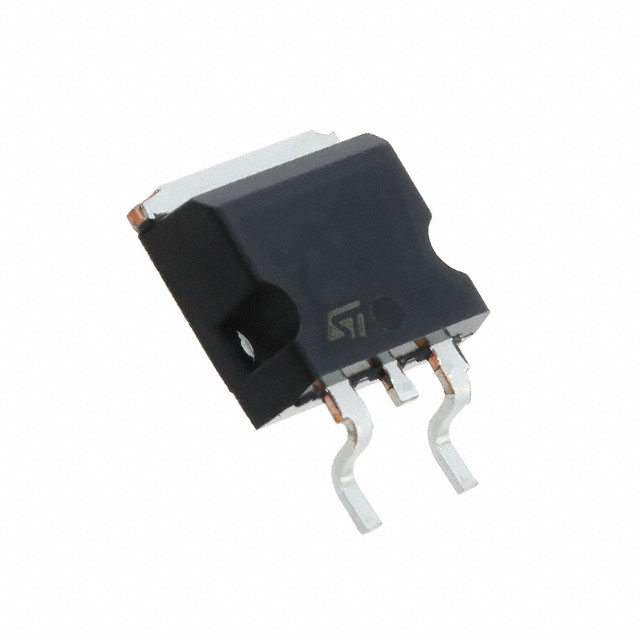
STB33N60DM2
Single FETs, MOSFETs

Not available to buy online? Want the lower wholesale price? Please Send RFQ to get best price, we will respond immediately


.png?x-oss-process=image/format,webp/resize,p_30)


STB33N60DM2 Description
STB33N60DM2 Description
The STB33N60DM2 is a high-performance MOSFET (Metal Oxide) from STMicroelectronics, designed for applications requiring high voltage and current capabilities. This N-Channel device features a drain-to-source voltage (Vdss) of 600V and a continuous drain current (Id) of 24A at 25°C, making it suitable for a wide range of power electronics applications.
STB33N60DM2 Features
- High Input Capacitance (Ciss): With a maximum input capacitance of 1870 pF at 100V, the STB33N60DM2 offers low gate charge (Qg) of 43 nC at 10V, enabling fast switching and reduced power consumption.
- Low On-Resistance (Rds On): The device boasts a maximum on-resistance of 130mOhm at 12A and 10V, ensuring efficient power transfer and minimizing power losses.
- Robust Voltage Ratings: The STB33N60DM2 can handle a maximum gate-source voltage (Vgs) of ±25V and a threshold voltage (Vgs(th)) of 5V at 250µA, providing flexibility in circuit design.
- Power Dissipation: Capable of dissipating up to 190W at the case temperature (Tc), this MOSFET is well-suited for high-power applications.
- Mounting Type: The surface mount design allows for easy integration into compact and dense electronic systems.
- Compliance and Environmental: The STB33N60DM2 is RoHS3 compliant and REACH unaffected, ensuring environmental responsibility and regulatory compliance.
STB33N60DM2 Applications
The STB33N60DM2 is ideal for applications where high voltage and current handling capabilities are required, such as:
- Power Supplies: Due to its high voltage and current ratings, the STB33N60DM2 is well-suited for power supply designs, including switching power supplies and battery chargers.
- Motor Control: The low on-resistance and high current capabilities make it an excellent choice for motor control applications, such as electric vehicles and industrial motor drives.
- Industrial Automation: The robust voltage and current ratings, along with the low gate charge, make the STB33N60DM2 suitable for industrial automation systems, including robotics and control systems.
Conclusion of STB33N60DM2
The STB33N60DM2 from STMicroelectronics is a powerful MOSFET designed for high-voltage and high-current applications. Its unique combination of low on-resistance, high input capacitance, and robust voltage ratings make it an excellent choice for power supplies, motor control, and industrial automation systems. With its compliance with environmental regulations and surface mount design, the STB33N60DM2 offers a reliable and efficient solution for demanding power electronics applications.
Tech Specifications
STB33N60DM2 Documents
Download datasheets and manufacturer documentation for STB33N60DM2
Product Change Notification 2024-03-05 (PDF) Product Change Notification (PDF) Related Parts


Shopping Guide


.png?x-oss-process=image/format,webp/resize,h_32)


©2025 ERSA Electronics Corporation.