
 German
 Japanese
 Portuguese
 Korea
Korea
 Mexico
 Dutch
Dutch


STMicroelectronics
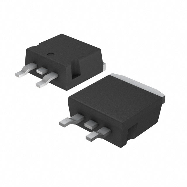
STB42N65M5

Why Choose Us?
Professional Platform
B2B & B2C purchasingDelivery at full speed
1-2 days deliveryWide variety
Original manufacturers365 days guarantee
Responsible quality
.png)


Tech Specifications
STB42N65M5 Description
STB42N65M5 Description
The STB42N65M5 from STMicroelectronics is a high-performance N-channel MOSFET designed for demanding power applications. With a 650V drain-to-source voltage (Vdss) and 33A continuous drain current (Id), it delivers robust performance in high-voltage circuits. The device leverages MDmesh™ V technology, optimizing switching efficiency and reducing conduction losses. Packaged in a D2PAK (TO-263) surface-mount format, it is suitable for automated assembly processes and offers excellent thermal management. Its low on-resistance (Rds(on)) of 79mΩ at 10V Vgs ensures minimal power dissipation, making it ideal for energy-efficient designs.
STB42N65M5 Features
- High Voltage & Current Rating: 650V Vdss and 33A Id (at 25°C) for robust power handling.
- Low Rds(on): 79mΩ @ 10V Vgs, enhancing efficiency in high-current applications.
- Advanced MDmesh™ V Technology: Reduces switching losses and improves thermal performance.
- High Drive Capability: Gate charge (Qg) of 100nC @ 10V ensures fast switching.
- Wide Vgs Range: ±25V maximum gate-source voltage for flexible drive circuitry.
- Thermal Resilience: 190W power dissipation (Tc) and 150°C junction temperature (TJ) rating.
- Reliable Packaging: D2PAK (TO-263) with RoHS3 compliance and MSL1 (unlimited) moisture sensitivity.
STB42N65M5 Applications
This MOSFET excels in high-efficiency power conversion systems, including:
- Switched-Mode Power Supplies (SMPS): Particularly in PFC (Power Factor Correction) stages.
- Motor Drives & Inverters: For industrial and automotive applications requiring high voltage tolerance.
- Renewable Energy Systems: Solar inverters and wind power converters benefit from its low-loss switching.
- LED Lighting Drivers: High efficiency and thermal stability make it suitable for high-power LED systems.
- DC-DC Converters: Where low Rds(on) and fast switching are critical for performance.
Conclusion of STB42N65M5
The STB42N65M5 stands out as a high-reliability MOSFET for 650V power applications, combining low conduction losses, fast switching, and excellent thermal performance. Its MDmesh™ V technology and D2PAK packaging make it a superior choice for designers prioritizing efficiency, power density, and durability. Whether in industrial motor drives, renewable energy systems, or high-efficiency SMPS, this MOSFET delivers consistent performance under demanding conditions.
FAQ
| Quantity | Unit Price | Ext. Price |
|---|---|---|
| 1+ | $20.75485 | $20.75 |
| 10+ | $19.83943 | $198.39 |
| 30+ | $18.25372 | $547.61 |
Not available to buy online? Want the lower wholesale price? Please Send RFQ to get best price, we will respond immediately


.png?x-oss-process=image/format,webp/resize,h_32)


