
 German
 Japanese
 Portuguese
 Korea
Korea
 Mexico
 Dutch
Dutch


STMicroelectronics
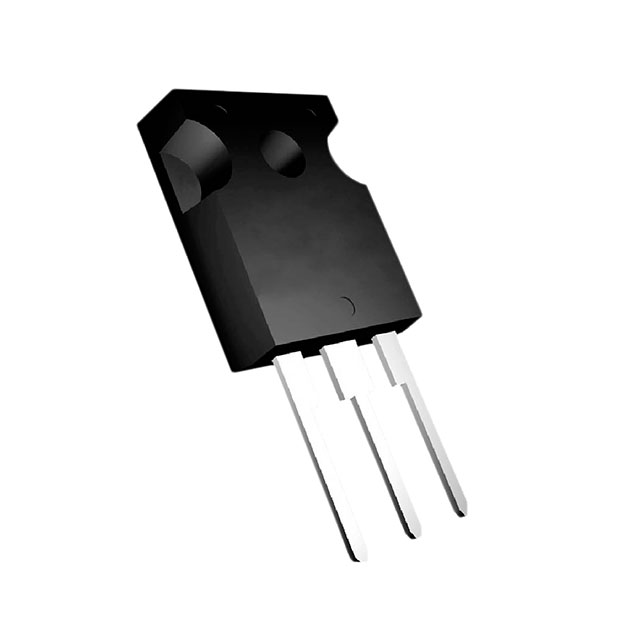
STF33N60DM2

Why Choose Us?
Professional Platform
B2B & B2C purchasingDelivery at full speed
1-2 days deliveryWide variety
Original manufacturers365 days guarantee
Responsible quality
.png)


Tech Specifications
STF33N60DM2 Description
STF33N60DM2 Description
The STF33N60DM2 from STMicroelectronics is a high-performance N-channel MOSFET designed for demanding power electronics applications. Built using MDmesh™ DM2 technology, it offers a robust 650V drain-to-source voltage (Vdss) rating and a continuous drain current (Id) of 24A (Tc). With an Rds(on) as low as 130mOhm @ 12A, 10V, it ensures efficient power handling with minimal conduction losses. The device features a low gate charge (Qg) of 43nC @ 10V and an input capacitance (Ciss) of 1870pF @ 100V, enabling fast switching performance. Packaged in a TO220FP through-hole format, it is suitable for high-power designs requiring thermal dissipation.
STF33N60DM2 Features
- High Voltage & Current Rating: 650V Vdss and 24A Id for robust power handling.
- Low On-Resistance: 130mOhm @ 12A, 10V for reduced conduction losses.
- Fast Switching: Optimized gate charge (43nC) and input capacitance for high-frequency operation.
- Thermal Efficiency: TO220FP package with 35W (Tc) power dissipation capability.
- Reliability: ROHS3 compliant, REACH unaffected, and MSL 1 (unlimited) moisture sensitivity.
- Wide Gate Drive Range: Supports ±25V Vgs(max) for flexible drive circuitry.
STF33N60DM2 Applications
The STF33N60DM2 is ideal for high-efficiency power conversion systems, including:
- Switched-Mode Power Supplies (SMPS): PFC stages, DC-DC converters.
- Motor Drives & Inverters: Industrial motor control, servo drives.
- Renewable Energy Systems: Solar inverters, wind turbine converters.
- UPS & Industrial Power Systems: High-voltage switching applications.
Its MDmesh™ DM2 technology provides superior switching performance and thermal stability compared to standard MOSFETs, making it suitable for high-frequency, high-power designs.
Conclusion of STF33N60DM2
The STF33N60DM2 combines high voltage capability, low Rds(on), and fast switching in a rugged TO220FP package. Its advanced MDmesh™ DM2 architecture ensures efficiency and reliability in demanding applications such as SMPS, motor drives, and renewable energy systems. With STMicroelectronics' proven quality standards, this MOSFET is a top choice for engineers seeking high-performance power switching solutions.
FAQ
Not available to buy online? Want the lower wholesale price? Please Send RFQ to get best price, we will respond immediately


.png?x-oss-process=image/format,webp/resize,h_32)


