
 German
 Japanese
 Portuguese
 Korea
Korea
 Mexico
 Dutch
Dutch


STMicroelectronics
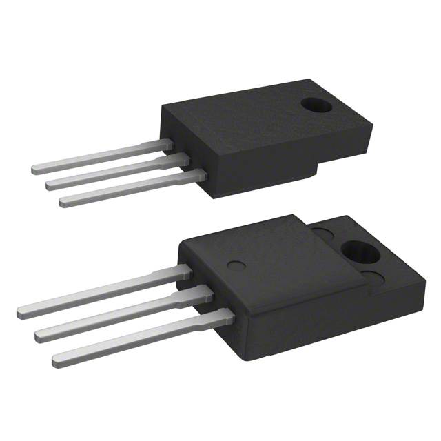
STF7N60M2

Why Choose Us?
Professional Platform
B2B & B2C purchasingDelivery at full speed
1-2 days deliveryWide variety
Original manufacturers365 days guarantee
Responsible quality
.png)


Tech Specifications
STF7N60M2 Description
STF7N60M2 Description
The STF7N60M2 is a high-performance MOSFET N-CH 600V 5A TO220FP from STMicroelectronics, designed for demanding applications that require high voltage and current handling capabilities. This device is part of the MDmesh™ II Plus series, known for its superior performance and reliability. With a maximum drain-to-source voltage (Vdss) of 600V and a continuous drain current (Id) of 5A at 25°C, the STF7N60M2 is well-suited for various power electronics applications.
STF7N60M2 Features
- High Voltage and Current Handling: The STF7N60M2 can handle a maximum drain-to-source voltage of 600V and a continuous drain current of 5A at 25°C, making it ideal for high-power applications.
- Low On-Resistance: With a maximum Rds(on) of 950mOhm at 2.5A and 10V, the STF7N60M2 offers low conduction losses, improving efficiency in power conversion systems.
- Robust Gate Drive: The device has a maximum gate-source voltage (Vgs) of ±25V, ensuring reliable operation in various gate drive conditions.
- Low Gate Charge: The maximum gate charge (Qg) is 8.8nC at 10V, contributing to fast switching speeds and reduced switching losses.
- Environmental Compliance: The STF7N60M2 is REACH unaffected and RoHS3 compliant, ensuring compliance with environmental regulations.
- Moisture Sensitivity Level (MSL) 1: This indicates that the device can be stored and handled without special precautions, simplifying logistics and inventory management.
STF7N60M2 Applications
The STF7N60M2 is ideal for a wide range of applications where high voltage and current handling are required, including:
- Power Supplies: In switch-mode power supplies (SMPS) and power factor correction (PFC) circuits, the STF7N60M2's high voltage and current ratings make it a suitable choice.
- Motor Control: The device's low on-resistance and robust gate drive capabilities make it suitable for motor control applications, such as in industrial automation and robotics.
- Battery Management Systems: In battery management systems for electric vehicles and energy storage, the STF7N60M2 can handle the high voltage and current requirements.
- Industrial Control: In industrial control systems, the STF7N60M2's ability to handle high voltage and current, along with its robustness, makes it an ideal choice for various control applications.
Conclusion of STF7N60M2
The STF7N60M2 from STMicroelectronics is a high-performance MOSFET that offers a combination of high voltage and current handling capabilities, low on-resistance, and robust gate drive. Its compliance with environmental regulations and moisture sensitivity level of 1 make it a versatile and reliable choice for a wide range of power electronics applications. With its unique features and advantages, the STF7N60M2 stands out as a preferred solution in demanding applications where performance and reliability are critical.
FAQ
| Quantity | Unit Price | Ext. Price |
|---|---|---|
| 1+ | $2.39143 | $2.39 |
| 10+ | $2.01600 | $20.16 |
| 50+ | $1.78115 | $89.06 |
Not available to buy online? Want the lower wholesale price? Please Send RFQ to get best price, we will respond immediately


.png?x-oss-process=image/format,webp/resize,h_32)


