
STMicroelectronics
STW56N65DM2
Single FETs, MOSFETs


.png?x-oss-process=image/format,webp/resize,p_30)


STW56N65DM2 Description
STW56N65DM2 Description
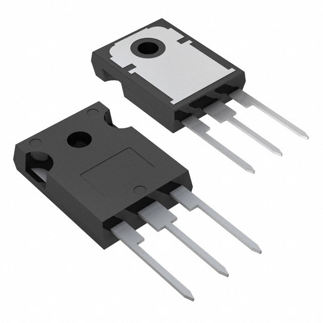
The STW56N65DM2 is a high-performance N-Channel MOSFET from STMicroelectronics, designed for applications requiring high voltage and current handling capabilities. With a drain to source voltage (Vdss) of 650V and a continuous drain current (Id) of 48A at 25°C, this MOSFET is ideal for use in power electronics applications. The device is manufactured using STMicroelectronics' advanced MDmesh™ DM2 technology, which provides superior performance and reliability.
STW56N65DM2 Features
- High Voltage and Current Handling: The STW56N65DM2 can handle a drain to source voltage of up to 650V and a continuous drain current of 48A at 25°C, making it suitable for high-power applications.
- Low On-Resistance: The device has a maximum on-resistance (Rds On) of 65mOhm at 24A and 10V, which helps reduce power dissipation and improve efficiency.
- Advanced MDmesh™ DM2 Technology: This technology provides improved performance, reliability, and thermal stability compared to traditional MOSFET technologies.
- Robust Gate Charge Characteristics: The STW56N65DM2 has a maximum gate charge (Qg) of 88nC at 10V, which helps reduce switching losses and improve overall efficiency.
- Compliance with Industry Standards: The device is compliant with the RoHS3 directive and REACH regulations, ensuring environmental and safety compliance.
- Through Hole Mounting: The STW56N65DM2 is available in a through-hole package, making it suitable for a wide range of applications and easy to integrate into existing designs.
STW56N65DM2 Applications
The STW56N65DM2 is ideal for use in various power electronics applications, including:
- Power Supplies: Due to its high voltage and current handling capabilities, the STW56N65DM2 is well-suited for use in power supply designs, such as SMPS (Switched-Mode Power Supplies) and DC-DC converters.
- Industrial Automation: The device's robust performance and reliability make it an excellent choice for use in industrial automation applications, such as motor drives and control systems.
- Renewable Energy: The STW56N65DM2 can be used in renewable energy applications, such as solar inverters and wind power systems, where high voltage and current handling are required.
- Electric Vehicles: The device's high performance and reliability make it suitable for use in electric vehicle applications, such as battery management systems and motor controllers.
Conclusion of STW56N65DM2
The STW56N65DM2 is a high-performance N-Channel MOSFET from STMicroelectronics, offering excellent voltage and current handling capabilities, low on-resistance, and advanced MDmesh™ DM2 technology. Its robust performance, compliance with industry standards, and through-hole mounting make it an ideal choice for a wide range of power electronics applications, including power supplies, industrial automation, renewable energy, and electric vehicles.
Tech Specifications
STW56N65DM2 Documents
Download datasheets and manufacturer documentation for STW56N65DM2
 Product Change Notification (PDF) PRODUCT CHANGE NOTIFICATION (PDF)
 Shopping Guide


.png?x-oss-process=image/format,webp/resize,h_32)


