
 German
 Japanese
 Portuguese
 Korea
Korea
 Mexico
 Dutch
Dutch


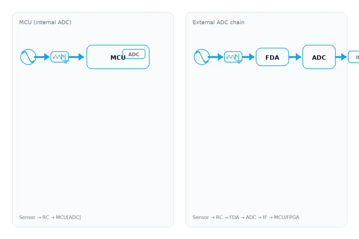
Do I need an external ADC if my MCU already has one?

Do I need an external ADC if my MCU already has one?
Also searched as “MCU ADC vs external ADC”.
Conclusion first: If your use case is ≤200 kSps, needs only ~≤12-bit effective resolution, and has no strict requirements for simultaneous sampling, isolation, or differential inputs, the MCU’s internal ADC is usually enough.
Switch to an external ADC if any applies: >1 Msps, >12-bit effective, tighter INL/DNL, differential/isolated front-end, simultaneous multi-channel, or interface bandwidth becomes a bottleneck.
What’s next: use the 30-second checklist below and see scenario mapping; deep dives are in the “Read next” cards.
Want to learn What is an ADC? Read the definition →
30-Second Decision
Check ≥3 on the left → stay internal; hit any one on the right → go external.
Use the MCU’s internal ADC if you meet most:
Choose an external ADC if any apply:
Reasons to use an external ADC
Use the quick checks below. If you match the “Good fit” or fail the “Quick check” for MCU ADC, moving to an external ADC is usually safer.
Higher performance
External converters deliver higher ENOB, faster sampling, and tighter linearity (INL/DNL) than typical MCU ADCs—critical in motor control, metering, or IF sampling.
Good fit: need >12-bit effective or >1 Msps; MCU readings plateau even after improving Vref/driver.
Read more →Specific features
Need differential inputs, wide common-mode, near-sensor PGA, or simultaneous sampling? External ADCs also support isolated front-ends for safety/noise.
Quick check: sensor common-mode falls outside MCU ADC range, or you need per-channel gain/sync.
Read more →Lower noise floor
With a low-noise Vref, proper driver/buffer, and correct anti-aliasing, an external chain suppresses PSU/ground-bounce that bleeds into codes.
Quick check: after decoupling and grounding fixes, code noise still >1–2 LSB at target bandwidth.
Read more →Deterministic timing
Pair with low-jitter clocks/PLLs and high-speed links so sampling instants/throughput are predictable. Interfaces like LVDS/JESD204/parallel prevent bus contention at high data rates.
Quick check: required throughput fs×bits×channels/efficiency exceeds MCU bus/DMA capacity or ISR jitter shows in codes.
Read more →Modular design
Reuse a proven module/eval board to reduce bring-up risk and tuning time. Let the external chain handle precision and throughput while the MCU focuses on control/UI.
Good fit: tight schedule, small team, or compliance testing ahead (fewer unknowns).
Read more →Reasons to stay with the MCU’s internal ADC
If your bandwidth and accuracy targets are moderate, the internal ADC keeps the design lean and fast to bring up. Use the checks below to confirm it’s a good fit before adding external silicon.
Lower cost / simpler BOM
No extra ADC IC, driver amp, precision reference, or clock tree. Fewer parts mean fewer supply risks and less assembly/debug surface—especially helpful in small-batch runs.
Good fit if: your target is ≤200 kSps and effective ≤~12-bit, and you value lead-time and simplicity over marginal performance gains.
Read more →Simpler firmware
Use timer-triggered conversions + DMA; no high-speed link drivers or external FIFOs to maintain. Fewer moving parts reduce integration bugs and shorten bring-up.
Quick check: at your target rate, ADC+DMA keeps CPU load <10% and ISR jitter doesn’t show up in measured codes.
Read more →Space / power savings
Internal ADCs minimize footprint and quiescent draw—ideal for IoT nodes and battery devices. You also avoid extra regulators, line drivers, and clock sources that radiate noise.
Good fit if: the board has tight area or sleep-heavy duty cycles where every µA matters.
Read more →Oversampling / averaging
With low-bandwidth signals, averaging reduces code noise ~√N and stabilizes readouts. It improves apparent resolution but not true ENOB, and returns diminish beyond moderate N.
Try first: N=16–64 averages; confirm the sensor bandwidth still meets spec and the UI latency is acceptable.
Read more →Bring-up Tips (quick checklist)
- If source impedance >10 kΩ, add a buffer amp so the sampling cap fully charges.
- Decouple Vref locally (10 µF ∥ 0.1 µF) and route digital returns away from the reference node.
- Schedule sampling on a timer right after quiet power periods; avoid motor/heater switching at that instant.
- Run a code-histogram: 95% of samples within ±1 LSB at your bandwidth ⇒ likely OK to stay internal.
Scenario Mapping: Pick Your Path
Match your application to the closest case below. Each card gives a decision, numeric hints, a common pitfall, and a single “Read next” route.
Temperature / battery / slow sensors (<10 kHz)
Decision: stay with the MCU’s internal ADC. Low bandwidth and relaxed linearity/sync make it the leanest path.
Hints: sampling ≤ 200 kSps, effective ≤ ~12-bit ENOB.
Pitfall: drift/jitter usually comes from Vref decoupling, ground return, or a missing RC—not the ADC silicon.
Strain / pressure / precision low-freq
Decision: use an external ΔΣ ADC for high resolution and strong out-of-band rejection.
Hints: target effective > 12-bit ENOB; bandwidth ≤ tens of kHz.
Pitfall: averaging smooths codes but does not raise true ENOB.
Motor control / energy metering
Decision: external ADC with simultaneous sampling and often isolation to keep phases aligned and safe.
Hints: hard limits on phase error/channel matching; safety or EMI requires isolation.
Pitfall: time-multiplexed MCU sampling skews electric-angle estimation.
Audio / acoustics
Decision: external ΔΣ ADC; jitter and filter response dominate perceived quality.
Hints: fs = 44.1/48/96/192 kHz; strict jitter and passband flatness.
Pitfall: ignoring master-clock jitter and anti-aliasing makes “extra bits” meaningless.
High-speed / IF sampling (MHz-class)
Decision: external Pipeline/Flash ADC and size the link first.
Hints: fs ≥ several Msps; analog BW ≥ tens of MHz; throughput = fs×bits×channels/eff.
Pitfall: ignoring protocol efficiency/overhead and MCU bus/DMA limits.
If you go external: 6-step integration checklist
Short, actionable steps. Each line ends with a single route for deeper guidance.
- Front-end: Sensor → AA RC → Buffer/Driver → ADC IN (match the sampling capacitor). Read next → Anti-aliasing
- Reference: low-noise Vref with local decoupling (10 µF ∥ 0.1 µF); keep digital return currents away. Read next → Front-End & Vref
- Clocking: choose low-jitter sources matched to target ENOB/rate; higher input frequency is more jitter-sensitive. Read next → Resolution / ENOB / SNR
- Interface: size throughput = fs × bits × channels / efficiency before picking SPI / LVDS / JESD204 / parallel. Read next → Interfaces
- Isolation / differential: select topology per common-mode and safety needs; prefer fully differential inputs with proper range. Read next → Front-End & Vref
- Layout: single-point AGND/DGND; keep sensitive traces away from high-current loops; run a code-histogram sanity check before release. Read next → Errors & Linearity
FAQ
Submit your BOM — get 3 safe options in 48 hours
We’ll shortlist three compatible ADCs with indicative lead time and price range, plus front-end/Vref and interface notes tailored to your build.
We support Cut-Tape / Partial Reel / AEC-Q.

Related Articles
- ·DDR4 vs DDR5 for Industrial Embedded Systems
- ·How to Choose Industrial DDR4 Memory for Medical Devices
- ·Memory Chip Price Increase: 2026 Market Trends, Samsung Pricing, Key Drivers and FAQ
- ·Memory Chip Manufacturers: Who Makes Memory Chips and Where
- ·Memory Chips: Materials, Applications, Types, and On-Chip Memory Explained
- ·Memory Chip Complete Guide: Definition, Manufacturers, Shortage, Manufacturing Process and Working Principles
- ·Fiber Optic Switch Guide: Definition, Connection Methods, Cabling, Disconnection and FAQ
- ·Optical Fiber Transmitter and Receiver Guide
- ·ICD Driver, LCD Driver & LCD Panel Driver Board Guide
- ·Touch Screen Overlay Guide for Commercial & Industrial Applications


.png?x-oss-process=image/format,webp/resize,h_32)


