
 German
 Japanese
 Portuguese
 Korea
Korea
 Mexico
 Dutch
Dutch


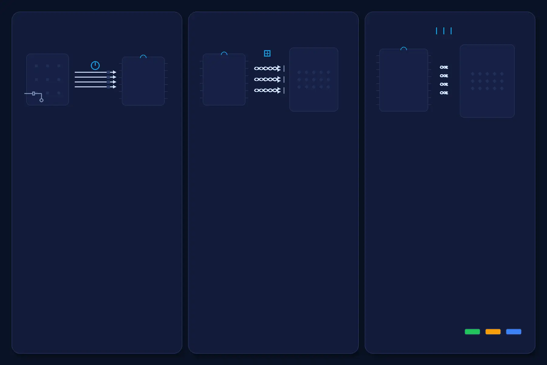
ADC Interfaces: SPI vs LVDS vs JESD204 — Which should I use?

Which ADC Interface Should I Use? SPI vs LVDS vs JESD204
Got fs, bits, channels, your host (MCU/FPGA), and need deterministic latency? Use the flow below to pick the right ADC interface.
- SPI — Simple and MCU-friendly; up to tens of Mbps; best for few channels / lower rates.
- LVDS — Mid-to-high speed, differential and source-synchronous; common on fast SAR/pipeline ADCs.
- JESD204 (B/C) — Very high throughput, multi-channel, deterministic latency, scalable; requires FPGA/SerDes.
Want to learn What is an ADC? Read the definition →
Quick Picker — Decision Flow & One-Line Math
Have answers to four quick questions? Follow them to a safe interface choice.
fs × bits × channels > ~30–50 Mbps?(JESD204 uses SYSREF and multi-lane alignment for deterministic latency.)
Example — 2ch × 14-bit × 5 MS/s ⇒ 140 Mbps raw; with 8b/10b ≈ 175 Mbps; +20% headroom ⇒ ≈ 210 Mbps → LVDS turf.
- SPI: Watch MCU SCLK ceiling and DMA; long or cross-board wires are risky.
- LVDS: Keep 100 Ω differential impedance, length match, and place termination correctly.
- JESD204: Calculate lane rate × lane count; Subclass/SYSREF drive determinism.
SPI — When to Use, Limits, Layout & Bring-up
3.1 When SPI makes sense
- Low / mid-speed capture, single or few channels; direct MCU connection.
- Prototype / small-batch builds need a fast bring-up with low BOM and tooling cost.
- Lightweight integration with firmware/GUI, no FPGA/SerDes required.
3.2 Throughput limits & safe margin
Quick estimate (SPI uses E_coding ≈ 1.00): Required SCLK ≈ (fs × bits × channels) / E_coding
- Leave 10–20% headroom for framing, alignment and device wait states.
- Typical MCU sustainable SCLK spans ~10–40 MHz (higher is possible but board routing, load and DMA overhead apply).
- Long runs / cross-board jumpers / noisy environments lower the practical SCLK ceiling.
Example: 16-bit × 1 ch × 500 kS/s → 8 Mbps raw; +20% headroom → ≈9.6 Mbps SCLK ⇒ SPI is feasible on many MCUs if routing is short and clean.
3.3 Layout — Do
- Keep traces short, continuous reference plane; ensure a clear clock return path.
- Place 22–47 Ω source series resistors on SCLK/MOSI near the driver to tame ringing/overshoot.
- Use proper near-receiver termination/mode per datasheet (pull-ups/downs, Schmitt options).
- Isolate from switchers/motors; if you split grounds, single-point tie near the ADC.
3.3 Layout — Don’t
- No long breadboard leads or ribbon cables for high-edge SCLK.
- Avoid casual level shifters between 1.8↔3.3 V — they add skew and edge distortion.
- Don’t meander CS/DRDY — sloppy routing eats setup/hold margins.
3.4 Bring-up checklist (step-by-step)
- Power & reference: verify Vref decoupling and ground bounce (scope the ripple).
- Probe the link at low SCLK: read the fixed device ID/version register first.
- Match SPI mode: set CPOL/CPHA per datasheet; confirm bit order (MSB/LSB).
- Code format sanity: apply a static step input and check Straight / Offset-Binary / Two’s-Complement decoding.
- Edge timing margin: raise SCLK gradually; measure MISO sampling window (LA/scope).
- DMA / ISR: enable circular DMA or double buffer; watch for overrun / dropped samples.
- Integrity checks: enable frame header/CRC/alignment flags if supported.
- Soak test: run 10–30 min under thermal/load variation; track code jitter and error counters.
3.5 Common pitfalls (symptom → fix)
- Waveform looks fine but codes are wrong: CPOL/CPHA or bit order mismatched to the timing diagram.
- Sporadic misalignment / lost codes: CS/DRDY setup/hold violated; SCLK edge too sharp → add series resistors.
- Random codes after long/cross-board runs: poor edge integrity → buffer, series damping, or move to differential.
- I/O domain mismatch: ADC and MCU voltage levels differ → use a proper same-domain pairing or a spec’d translator.
3.6 When NOT to use SPI
- When
fs × bits × channelsapproaches or exceeds your MCU’s sustainable SCLK (incl. DMA overhead and 10–20% headroom). - When you need deterministic latency or multi-device sync (→ prefer JESD204).
- When routing is long or EMI is heavy and you can’t guarantee edge integrity (→ prefer differential LVDS/JESD).
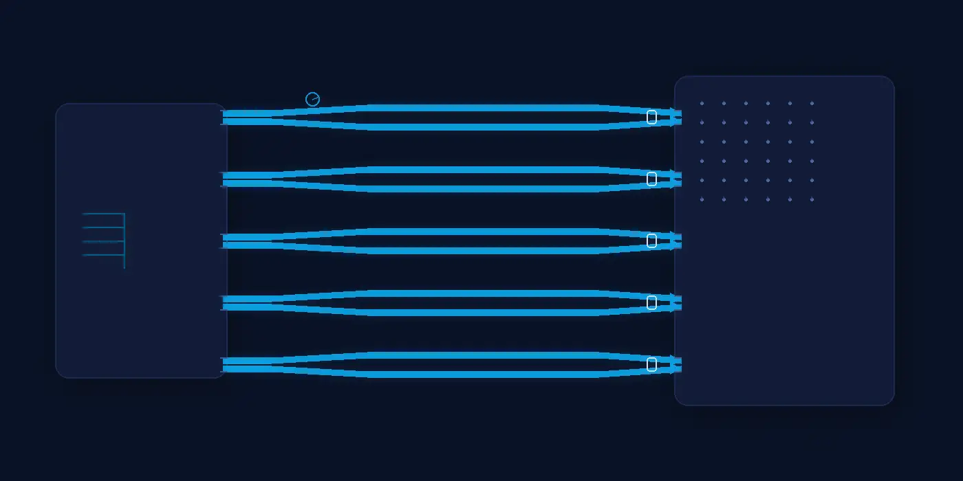
LVDS — Differential, Source-Synchronous, Mid-to-High Speed
4.1 When LVDS fits
- Tens to hundreds of Mbps per pair; parallel data pairs (often DDR) for aggregate throughput.
- Differential noise immunity and lower emissions; better for longer on-board runs or noisy environments.
- Source-synchronous capture (forwarded DCO + DATAx) is friendlier than MCU-sampled SPI at these rates.
4.2 System shape
ADC forwards a differential clock (DCO+/−) plus one or more DATA+/− pairs (often DDR). The receiver (FPGA or dedicated LVDS RX) performs bit/word alignment per channel, then buffers to FIFO/processing. No heavy line coding (usually no 8b/10b), but frame/word markers may exist.
4.3 Throughput & lane math (one-liners)
T_raw = fs × bits × channelslane_rate ≈ T_raw / N_pairs(LVDS coding efficiency ≈ 1.00)- For DDR data:
f_DCO ≈ lane_rate / 2 - Unit interval:
UI = 1 / lane_rate; keep intra-pair skew ≲ 10–20% UI. - If the ADC uses a serializer factor S (e.g., 7:1/14:1), compute N_pairs and f_DCO per the datasheet mapping.
4.4 Layout — Do
- Route 100 Ω differential pairs, tightly matched length; control intra-pair skew within your UI budget.
- Maintain a continuous reference plane; pre-plan return paths when crossing layers or plane splits.
- Place termination at the receiver (or enable internal 100 Ω) close to pins.
- Use paired vias, minimize stubs (back-drill/blind-buried if needed).
4.4 Layout — Don’t
- No test pads/fly-wires inside a pair — they create stubs.
- Avoid crossing plane splits or running parallel to noisy switching rails.
- Don’t mismatch pair lengths or swap P/N; both collapse eye opening.
4.5 Bring-up checklist
- Lock DCO & data: verify DCO frequency/duty and DDR relationship to DATAx (scope/LA/ILA).
- Frame/word alignment: enable the device’s align mode or implement bit-slip/word-align in the FPGA.
- Lane matching: align channels (bit/word) and measure lane-to-lane skew.
- Jitter margin: check sampling edge margin; tune input delay/phase on the FPGA; reduce on-board noise sources if needed.
- Integrity checks: run known patterns (fixed/step codes) and track error/lost-frame indicators.
- Soak test: 10–30 min over temp/load; ensure no intermittent misalignment.
4.6 Common pitfalls
- P/N swaps or pair crossovers → inverted/garbled codes.
- No/incorrect termination or wrong location → amplitude issues, crosstalk/EMI rise.
- Excessive intra-pair or lane-to-lane skew → collapsed eye, random bit errors.
- Poor DCO duty/jitter → reduced sampling window, intermittent faults.
4.7 When to step up to JESD204
- More channels or rising aggregate throughput demanding scalability.
- Off-board/cable links or deterministic latency and system-wide synchronization.
- Planned lane aggregation or distributed acquisition architectures.
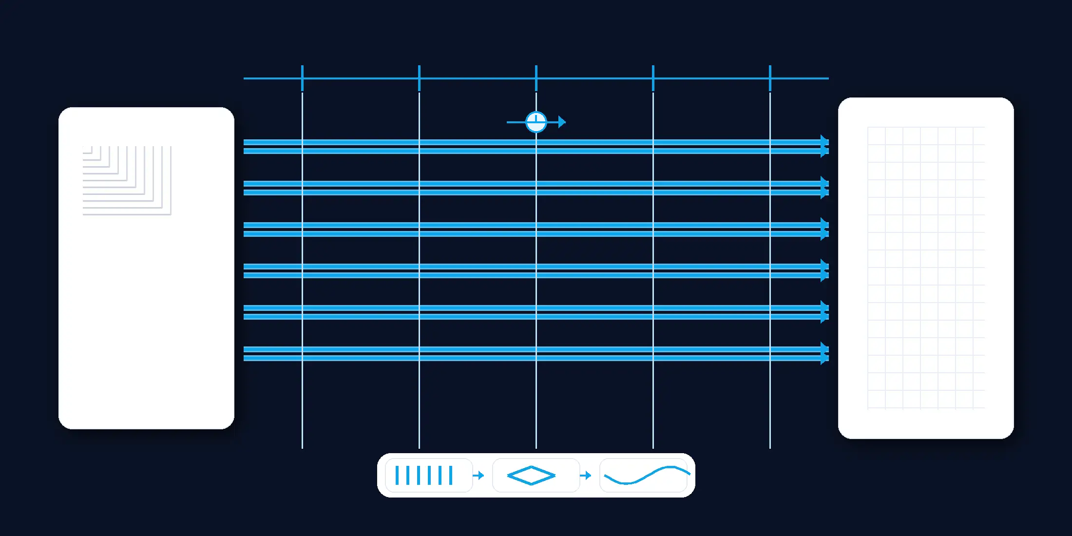
JESD204 (B/C) — Ultra-High Throughput, Multi-Channel, Deterministic
5.1 When JESD204 makes sense
- Very high aggregate throughput and/or many channels beyond LVDS comfort.
- Deterministic latency and fleet-wide synchronization needs (Subclass with SYSREF/LMFC).
- Scalable multi-lane SerDes links; typical host is an FPGA/SoC with SerDes.
5.2 Concepts at a glance
- Multi-lane SerDes aggregates throughput; trade lane rate vs lane count.
- Link bring-up stages: CGS → ILAS → DATA.
- Determinism: SYSREF/LMFC (Subclass) for fixed, repeatable latency and device alignment.
- Coding efficiency: 8b/10b ≈ 0.80; 64b/66b ≈ 0.97 (JESD204C supports higher efficiencies and rates).
5.3 Lane-rate math (one-liners)
Tip — Plan lane-to-lane skew and LMFC alignment windows when choosing N_lanes.
5.4 Layout & clocking — Do
- Route controlled-impedance differential pairs, matched length, continuous return paths.
- Use paired vias, keep stubs minimal (back-drill where needed).
- Distribute low-jitter clocks and SYSREF symmetrically; document LMFC relations.
- Mind PI/SI: SerDes rail decoupling, plane integrity, isolation from RF/analog front-ends.
- Simulate eye/channel if possible (CTLE/DFE/pre-emphasis budgeting).
5.4 Layout & clocking — Don’t
- Don’t cross plane splits or run near switching/high-current paths.
- Don’t treat SYSREF as a casual GPIO; asymmetry kills determinism.
- Don’t place test pads near SerDes pins; avoid return-via omissions.
5.5 Bring-up checklist (CGS → ILAS → DATA)
- Clock & SYSREF up: verify ref-clock jitter, SYSREF edges, and LMFC phase relations.
- CGS: achieve code-group sync; confirm character alignment stability.
- ILAS: exchange parameters; match lane IDs, octets, scrambling, subclass.
- DATA: enable lane alignment/deskew; align all lanes to the same LMFC.
- Determinism: measure end-to-end latency; confirm cross-reset repeatability.
- Error monitors: track bit/frame/multiframe errors; stress temp and supply noise.
5.6 Common pitfalls
- SYSREF/LMFC mis-config or asymmetric routing → no determinism or drift across resets.
- Mismatched coding/mapping (8b/10b vs 64b/66b, scrambling, F/K characters) → CGS/ILAS loops.
- Excessive lane skew → lanes won’t align; intermittent bit errors.
- Poor PI/SI → eye closure, rising BER; SerDes rail ripple causes wander.
5.7 When NOT to use JESD204
- Your host is MCU-only (no SerDes/FPGA capability).
- Aggregate throughput and channel count are modest (SPI/LVDS suffice).
- Strict cost/power budgets rule out SerDes and clock-tree complexity.
Practical Patterns — From Requirements to Interface
FAQ — Interface Selection

Related Articles
- ·HBM3 vs. HBM3E: Complete Technical Comparison for AI, HPC, and Global Component Procurement
- ·How Large Language Models Work
- ·SK Hynix & Samsung: The Unprecedented HBM Expansion Race
- ·Micron 6600 ION 245TB Redefines Data Center
- ·Why Memory and Storage Define the Next Decade
- ·How Artificial Intelligence Acquires “Knowledge”
- ·How DRAM Will Change the World
- ·Why SSD Write Cache Is Crucial for AI Applications
- ·DRAM Product, Technology & Application Guide
- ·HBM4 compared to HBM4E


.png?x-oss-process=image/format,webp/resize,h_32)


