
 German
 Japanese
 Portuguese
 Korea
Korea
 Mexico
 Dutch
Dutch


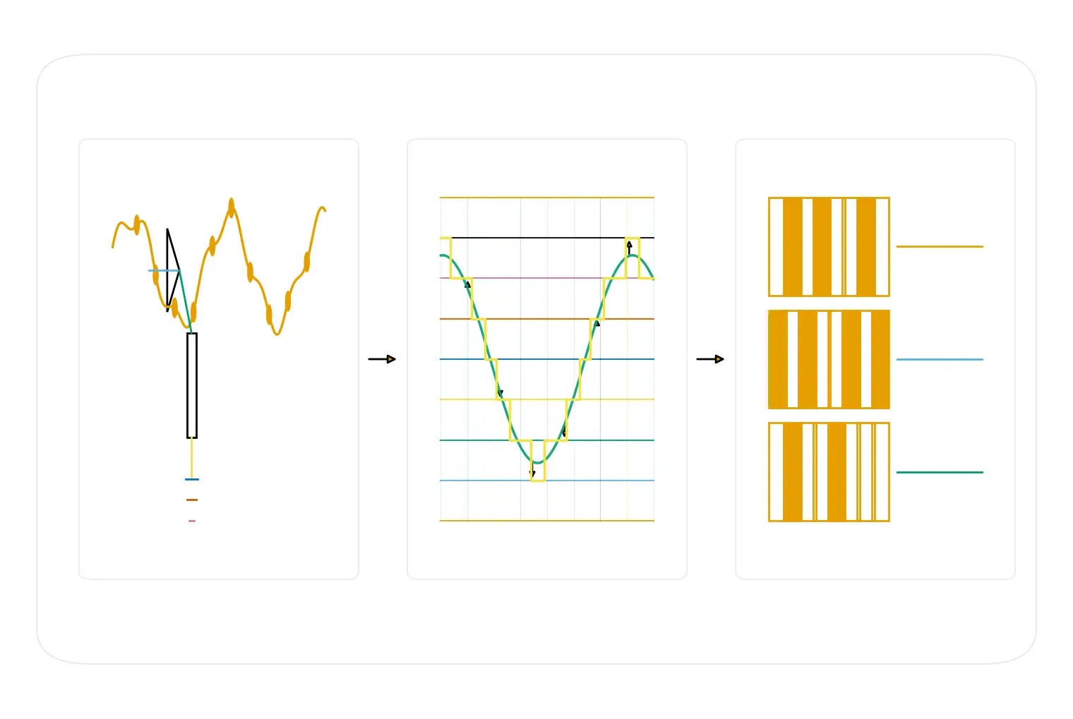
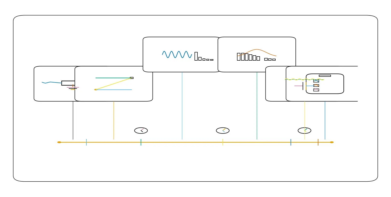
How to Convert Analog to Digital: Step-by-Step

How to Convert Analog to Digital (Correctly)
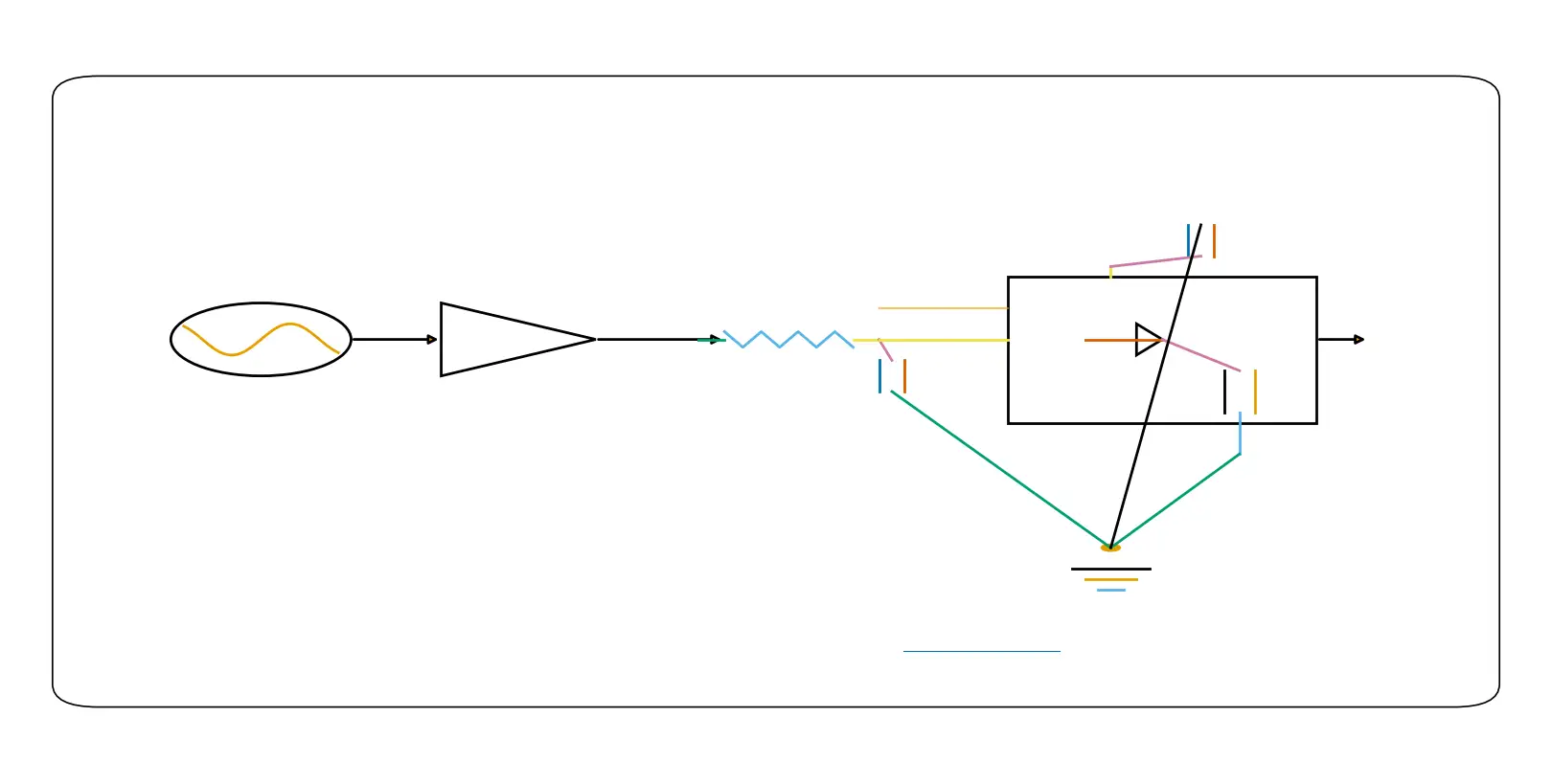
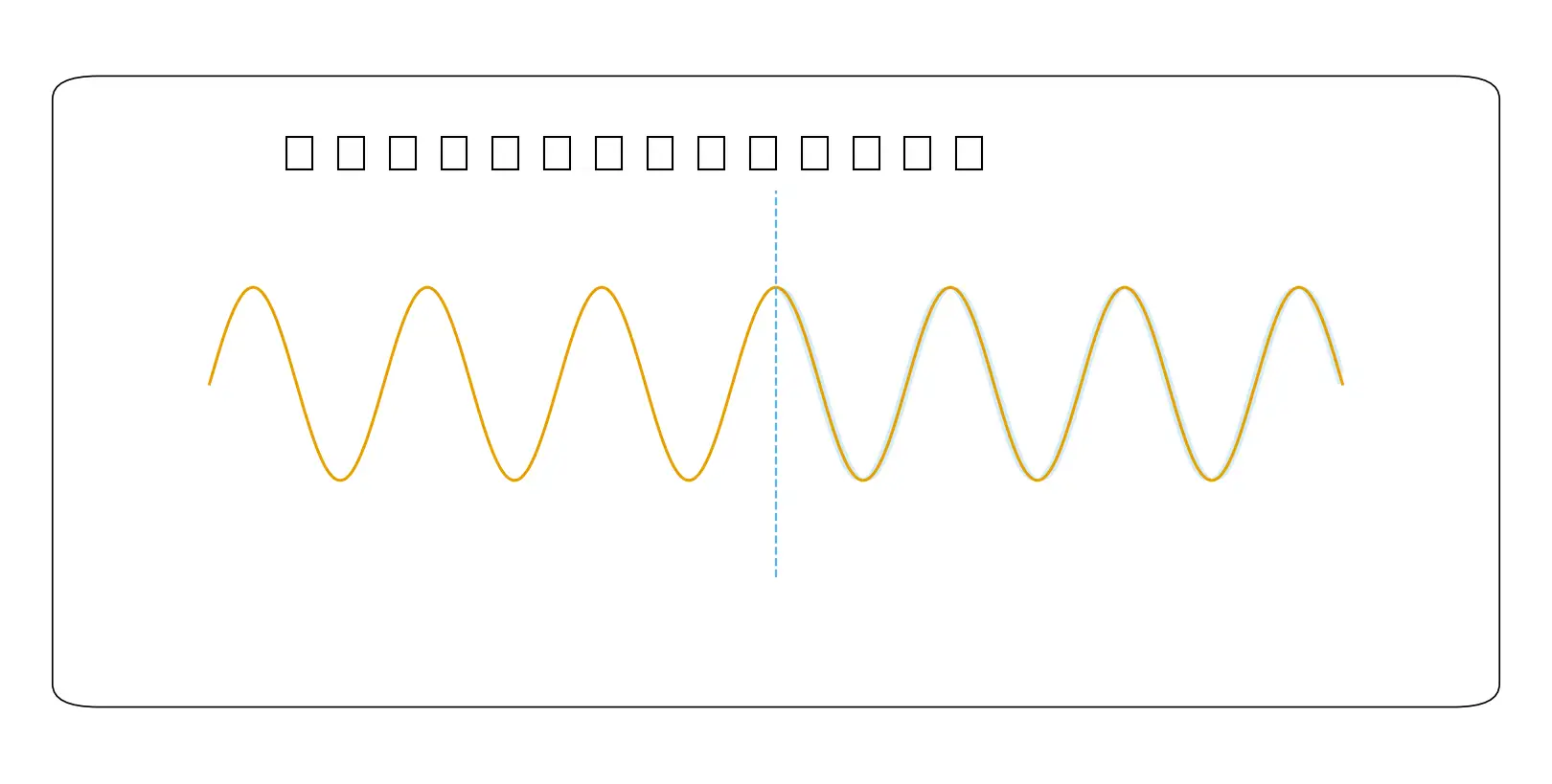
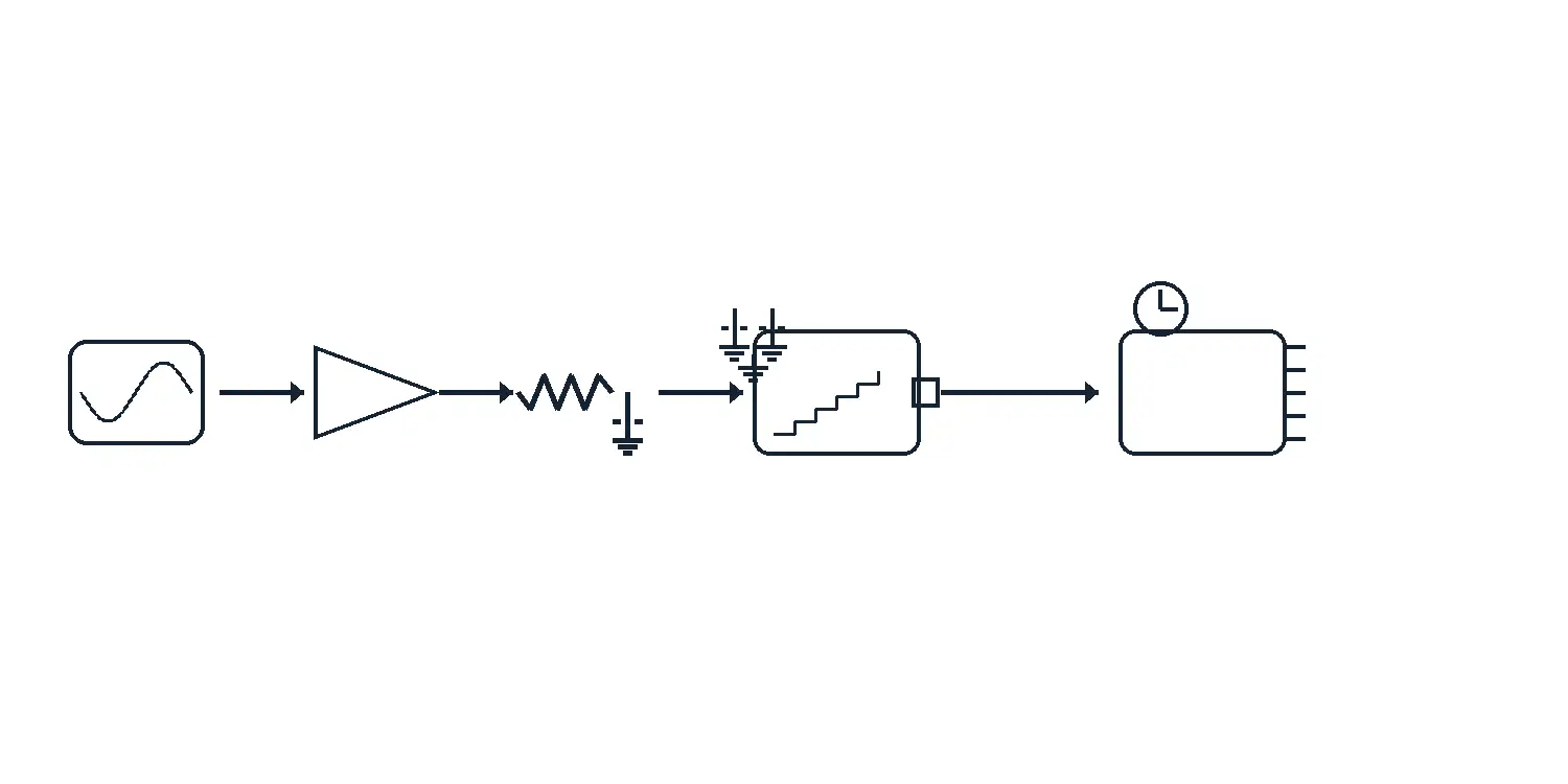
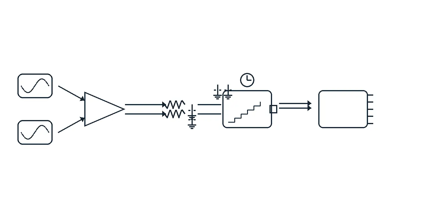
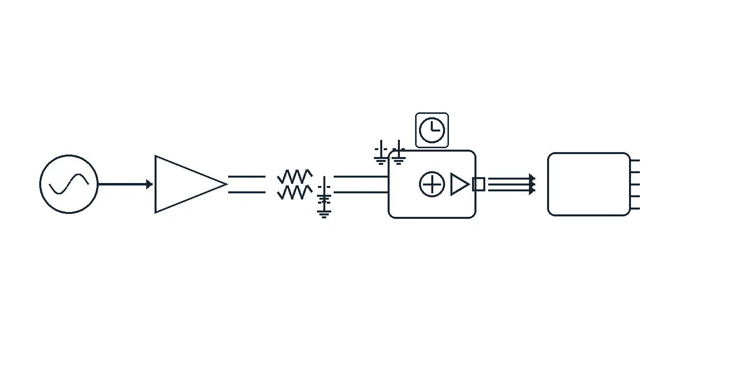
Converting analog to digital follows three clear steps. Sampling takes time-aligned snapshots of the signal at a fixed rate. Quantization rounds each snapshot to the nearest discrete level. Coding then represents that level as a binary number your MCU/FPGA can read. Below we give safe defaults (sampling rate, anti-alias filter, drivers, Vref) and a 10-minute bring-up check so small-batch builds just work. Want “What is an ADC?” Read the definition →
Step 1 — Define the Signal & Goals
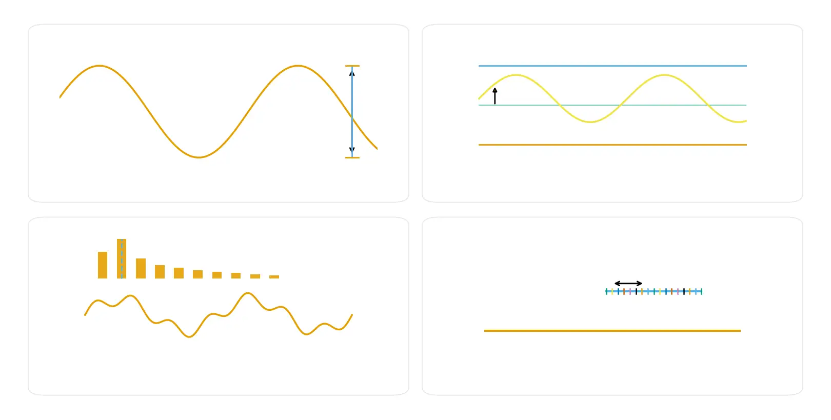
Before filters or ADC choice, write down four facts about the signal—amplitude, DC offset, highest effective frequency (fmax), and dynamic range / required resolution. This sets the engineering bounds for every step that follows.
Pressure sensor 0–4 V with 2 V bias; care about ~800 Hz content ⇒ take fmax≈1 kHz; smallest change ≈2 mV ⇒ start at 12–14 bit. Choose fs=2.5–5 kHz. Source 5 kΩ ⇒ add buffer (lower source impedance for S/H).
Resolution vs dynamic range (rule-of-thumb): 12-bit ≈ 74 dB, 14-bit ≈ 86 dB, 16-bit ≈ 98 dB. If your smallest meaningful change is ~1/1000 of full-scale, ≥10–12 bit starts to make sense.
Finding fmax: for narrowband signals, use the top of the useful band; for pulses/fast edges, treat the steepest edge as high-frequency content.
Offset & window: confirm the ADC’s input common-mode window and polarity (unipolar/bipolar); shift the signal if needed.
- Chasing the datasheet maximum sampling rate while ignoring the useful bandwidth and anti-alias headroom.
- Forgetting DC offset / common-mode → codes look “valid” but map to the wrong window.
- No budget for temp drift / Vref noise / ground bounce—pursuing high resolution that the layout/power can’t support.
- Do you have Vmin…Vmax, Vcm, fmax, and the smallest meaningful change written down?
- Is fs ≥ 2.5× fmax?
- Is ADC-seen input impedance ≥ 10× source? If not, plan a buffer/driver.
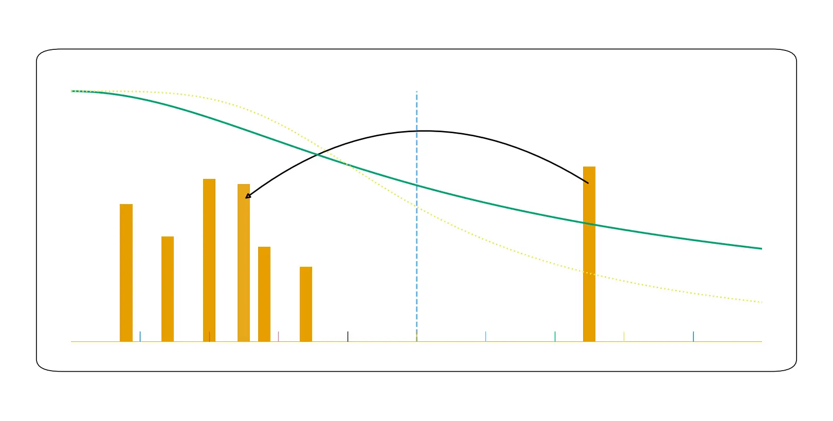
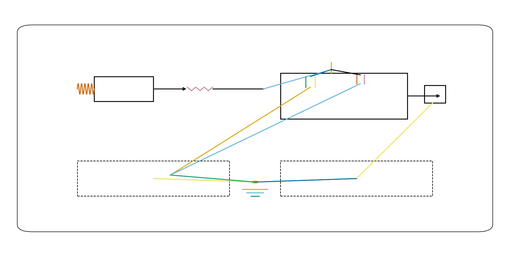
Step 2 — Anti-Aliasing & Front-End Filter
Aliasing reminder: anything above half the sampling rate (fs/2, Nyquist) folds back into baseband as a realistic-looking but false tone. Once sampled, no digital filter can restore it.
Where to place the filter: for single-ended signals, use a series R and a shunt C to ground. If you buffer, put the RC after the buffer and before the ADC IN. For differential inputs, use symmetrical RC on both legs and maintain common-mode. Keep the capacitor’s return at a clean local ground near the ADC (avoid split-plane crossings).
Mind the ADC’s sample-and-hold: too large a series R can prevent the internal sampling capacitor from charging within the aperture/hold window.
- Relying on digital filtering to fix aliasing—once folded, it cannot be undone.
- Putting the RC at a far location (edge of the board/probe side), letting the trace pick up new noise and spikes.
- Choosing an overly large series R so the S/H capacitor never fully charges; or using the wrong capacitor dielectric for stability.
- Sweep a sine toward fs/2 and compare spectra: with vs without RC, alias peaks should drop clearly.
- Feed a square/pulse and observe edge rounding; if high-frequency “texture” remains in codes, reduce fc (e.g., 0.3×fs) or go 2nd-order.
- Re-check the S/H charge time constant vs your sampling aperture/hold; adjust series R or add a buffer.
Step 3 — Choose ADC Architecture & Resolution
- Low–mid speed, general accuracy → choose SAR. (Often built into MCUs; simple, low latency.)
- High dynamic range / audio-grade linearity → choose ΔΣ. (Oversampling + digital filtering; tolerate latency.)
- High bandwidth, ultra-low latency → choose Pipeline/Flash. (Higher power/cost; FPGA-friendly interfaces.)
- SAR: low power & latency; needs low source impedance/driver for S/H; performance tied to clean Vref/layout.
- ΔΣ: excellent linearity & dynamic range; bandwidth/latency set by digital filter; jitter/reference noise reduce ENOB.
- Pipeline/Flash: extreme speed & low latency; higher power/cost; strict clocking/layout; interfaces often FPGA-oriented.
- ΔΣ for tight closed-loop control (ms/µs latency budget) → not suitable.
- SAR with high source impedance and no buffer at high sampling rates → likely distortion/settling issues.
- Pipeline when budget/power are tight but bandwidth demands are modest → overkill risk.
- Is your priority dynamic range/linearity or bandwidth/latency?
- What latency can the system tolerate (ms vs µs)?
- Can the front-end drive the chosen ADC (low source impedance, adequate GBW)?
- Do target bits align with realistic ENOB/SNR given Vref and noise budget?
Step 4 — Driver & Input Matching
An ADC isn’t an ideal voltmeter—the sample-and-hold (S/H) capacitor draws current during the sampling aperture. Without a proper driver and input match, you’ll see under-settling, distortion, or outright clipping.
Make sure energy actually arrives: the source + Rseries and the ADC’s internal S/H capacitor form a time constant. It should settle within the sampling aperture to well below a fraction of an LSB—higher source impedance demands a stronger driver and/or smaller Rseries.
Common-mode & input window: confirm polarity (unipolar/bipolar) and the allowed common-mode range. Apply bias/shift after the buffer so that the instantaneous sampling voltage always stays in range.
Stability: the driver + RC can ring; slightly increase Rseries or add a small output cap (pF-level) if you see overshoot.
- Clamp & limit: Rseries + diodes to AVDD/AGND (or Schottky to a reference rail) to absorb transients/over-voltage.
- EMI/ESD: consider TVS / RC snubbers at the connector; keep return loops tight near the ADC analog ground.
- Layout: shortest path from RC to ADC pin; capacitor returns to a clean local ground (avoid split-plane crossings).
- High source impedance driving a fast SAR → S/H never fully charges; distortion and INL/THD degrade.
- No input protection → probe/plug transients punch the ADC pin beyond rails.
- Common-mode out of range (VOCM mis-set on differential inputs) → codes look “valid” but are biased or clipped.
- Before power-on: VOCM, supply rails, and input window verified? RC located right at the driver/ADC with a clean local ground return?
- Step test: feed a small step/square; watch for under-settling or ringing in codes—reduce Rseries, increase driver GBW, or move to a 2nd-order RC if needed.
- Sine sweep: raise frequency/amplitude; check for clipping and rising THD—if present, revisit source impedance and bias window.
Step 5 — Reference (Vref) & Decoupling
The reference is the ruler for every code. If Vref is noisy or drifting, effective resolution collapses—even when sampling and front-end are correct.
Supply & topology:
- MCU internal ADC: start with the internal reference; upgrade to an external 2.5 V/4.096 V reference if noise/linearity demand it. Still place 10 µF ∥ 0.1 µF near Vref/Vdda.
- External ADC: reference IC → (optional small R/FB bead if allowed) → Vref pin. Use differential reference where supported for better PSRR.
Placement & parts: 0.1 µF = C0G/NP0; 10 µF = X7R. Keep caps adjacent to the pin, same layer, with a tight return to AGND. Keep references away from hot/noisy switchers and clocks.
- Ripple at Vref pin: < 10 mVpp as a minimum bar for 12-bit designs (tighten for higher resolution).
- Startup: wait for the reference to settle (datasheet ms-scale) before calibration/measurement.
- Code histogram: with a static input, distribution should be tight with no odd missing-code gaps.
- Sharing USB/digital rails for Vref — ripple and spikes map straight into LSBs.
- Decouplers placed far away or returning across split planes — large loop inductance → jitter and coupling.
- Ground bounce from digital high-current paths contaminating the analog reference loop.
- Are 10 µF ∥ 0.1 µF on the same layer right next to Vref, with a short return to AGND?
- Is Vref sourced from a clean LDO/reference (not a noisy digital rail), and tied to DGND only at a single point?
- Scope the Vref pin: ripple < 10 mVpp? No switching texture? If not, fix supply/placement before chasing higher ENOB.
Step 6 — Sampling Clock & Jitter
High-frequency inputs are extremely sensitive to clock jitter: more RMS jitter → lower SNR/ENOB. To keep effective bits, prioritize a clean clock source and disciplined routing.
Jitter-limited SNR follows SNRjitter ≈ −20·log10(2π·fin·σt). Use these total RMS jitter targets to roughly preserve ENOB:
- At 100 kHz input: 12-bit ≲ 320 ps, 14-bit ≲ 80 ps, 16-bit ≲ 20 ps.
- At 1 MHz input: 12-bit ≲ 32 ps, 14-bit ≲ 8 ps, 16-bit ≲ 2 ps.
Total jitter = √(source² + distribution/buffer² + ADC aperture²). Fix the source first.
- Assuming digital filtering can recover jitter loss — it cannot; jitter corrupts the sampling instant.
- Using an MCU PLL as the primary sample clock without dedicated clean power/decoupling.
- Clock traces that cross split planes or meander near Vref/analog paths, increasing phase noise and coupling.
- Before power-on: clock source on a clean LDO with local 10 µF ∥ 0.1 µF? Traces short, no plane crossings, proper terminations?
- After power-on (sine sweep): increase fin; if SNR drops earlier than expected, swap to a lower-jitter XO/module and re-check.
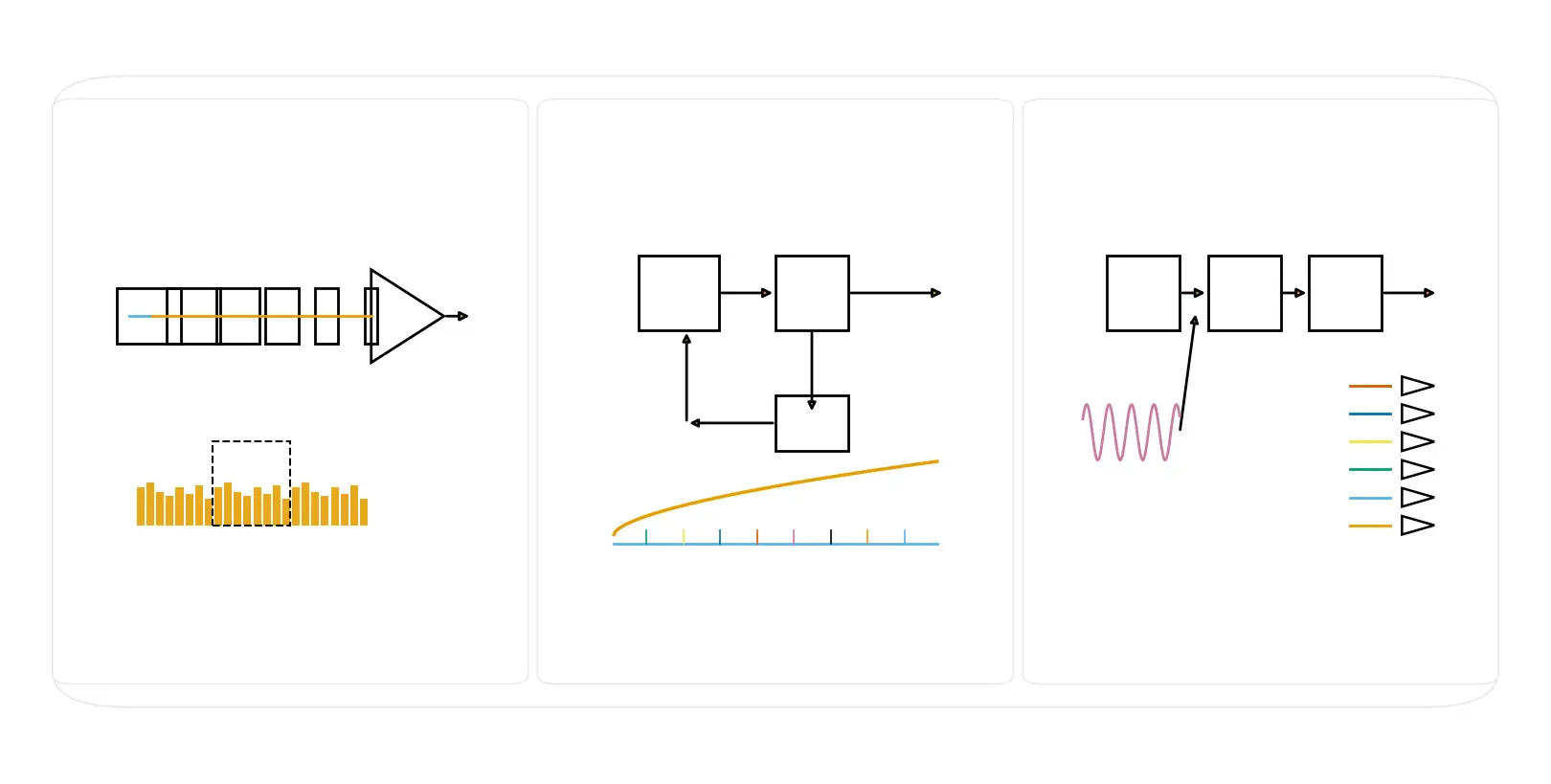
Step 7 — Interface Readout & MCU Variant
With the front-end and sampling in place, the last mile is moving codes reliably into your controller or FPGA. First size the throughput, then pick and wire the interface, and finally confirm the code format.
throughput ≈ bits × channels × fs / efficiency
- bits = effective frame width per sample (include status/alignment bits if present).
- channels = simultaneous channels (account for interleaving rules).
- fs = per-channel sampling rate.
- efficiency = protocol & framing overhead (typ. 0.6–0.95 for real sustained streaming).
Compare the result to your MCU/FPGA’s sustained link limits (SPI mode/CS gaps/DMA service time), not just headline MHz.
- Continuous DMA stream & circular buffers; minimize CS toggles & gaps.
- Match CPOL/CPHA to ADC edge; verify MSB/LSB and left/right alignment.
- Keep lines short; add small series terminations (10–33 Ω) at the source if needed.
- Respect lane mapping & frame/clock alignment.
- Differential pairs length-match; continuous reference plane; proper termination.
- Good for higher throughput with fewer pins and lower noise.
- Account for coding losses (8b/10b or 64b/66b) in efficiency.
- Implement SYSREF/LMFC deterministic latency alignment.
- Best with FPGAs for multi-channel high-speed capture.
- Lock to the ADC’s frame header/status bits; verify channel order for interleaved streams.
- Use FIFO/DMA with a circular buffer. Size guard-band:
buffer_bytes ≈ throughput (B/s) × guard_time (s). - Prefer hardware timers to trigger conversions for stable time-base.
- Single-ended: Sensor → RC → Buffer → ADC_IN; small series R (10–100 Ω) before S/H.
- Differential (if supported): Symmetrical RC + differential driver; set common-mode per datasheet.
- Code formats:
- Straight (natural): read as unsigned.
- Offset-Binary: convert to signed:
signed = code − 2^(N−1). - Two’s-Complement: ensure sign-extension and correct left/right alignment; confirm MSB-first.
- Data movement: use DMA (circular). Interrupts handle watermarks/flags only; avoid CPU polling.
- Oversampling/Averaging: reduces noise but changes data rate/bandwidth — include in throughput budgeting.
- Using headline link MHz without sustained throughput budgeting → dropped samples.
- Wrong SPI mode/edge, bit order, or alignment → shifted/unstable codes.
- Misreading code format (Offset-Binary vs Two’s-Complement) → polarity/zero offset errors.
- No FIFO/DMA → CPU stalls cause intermittent data loss, especially multi-channel.
- Multi-channel interleave channel order not verified → cross-talk misinterpretation.
- Before power-on: compute
bits × channels × fs / efficiency, compare to sustained link limits, leave 20–30% headroom. - SPI: confirm CPOL/CPHA, bit order, alignment, frame length; pre-configure DMA circular buffer.
- After power-on: logic analyzer one frame — verify header, bit order, frame length, channel order.
- Feed a ramp/step: check monotonicity and correct sign/zero; toggle oversampling to confirm expected throughput/noise change.
Step 8 — Quick Calibration & 10-Minute Self-Check
Validate that Steps 1–7 actually come together. In ten minutes you’ll verify zero/full-scale, aliasing, distortion/jitter, missing codes, and Vref health—then record a go/no-go.
- DMM (for rails/offsets), oscilloscope (probe Vref ripple directly at the pin)
- Signal generator (sine & step), known reference (short/precision divider/reference IC)
- Logic analyzer (optional, to confirm frame/header/bit order)
- Ground/common-mode per datasheet; VOCM set (diff ADCs).
- Vref decouplers at pin (10 µF ∥ 0.1 µF); AGND/DGND single-point tie.
- Sampling clock present; interface idle without errors.
- Action: short input or apply a known reference (0 V / Vref/2 / near full-scale).
- Pass: zero within ±2–3 LSB; full-scale not clipped; monotonic ramp.
- If fail: offset → check bias/common-mode/Vref; clipping → input window/driver.
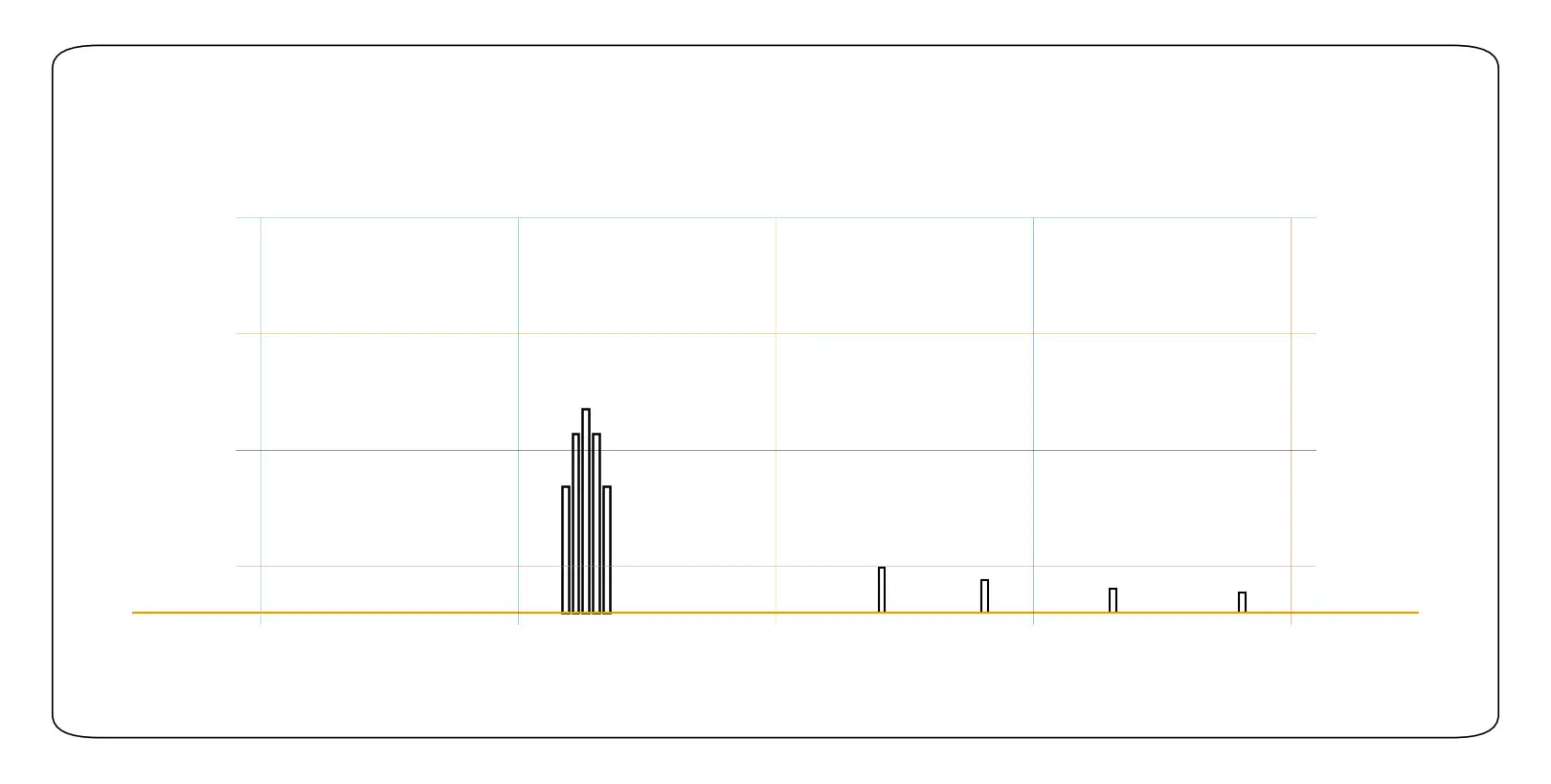
- Action: inject single tone; capture ≥4k samples; FFT or spectral view.
- Pass: clean main lobe; no obvious alias peaks; THD ≳ −60 dB (12-bit baseline).
- If fail: aliasing → Anti-alias; distortion → source impedance/driver/RC/GBW; early SNR drop → clock jitter.
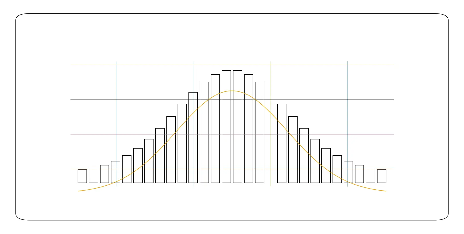
- Action: feed a stable DC or stepped input; build a code histogram (bin auto or 2N/16~2N/8).
- Pass: tight distribution, no missing codes, no weird double peaks; shorted-input width σ ≲ 0.5–1 LSB.
- If fail: missing codes/steps → INL/DNL/under-settling; excessive width → Vref noise/ground bounce.
- Action: scope directly at the Vref pin (short ground lead).
- Pass line: Vref ripple < 10 mVpp (12-bit+ starting point; tighten for higher resolution).
- If fail: move decouplers next to the pin, fix ground return, isolate from USB/noisy rails, use a low-noise LDO/reference.
- Log: zero/full-scale offset (LSB), SNR/THD, aliasing seen?, histogram notes, Vref ripple, any interface drops.
- If any item fails, jump to the corresponding step/page below.
Step 9 — Safe Recipes (Examples)
Not sure where to start? Use one of these safe starter recipes to light up your build. Tweak later after you verify bandwidth, noise, and codes with the 10-minute self-check.
Temperature / pressure / position sensing; low-power logging.
- Sampling: fs = 2.5–5 kHz (≥ 2.5× fmax).
- Filter: 1st-order RC, fc ≈ 0.4× fs, parts placed next to driver/ADC.
- Resolution: 12–14-bit start.
- Driver: single-ended buffer if source ≥ 5–10 kΩ; series R before S/H = 10–100 Ω.
- Vref: local decoupling 10 µF ∥ 0.1 µF; clean LDO or internal ref.
- Clock: board crystal or MCU timer trigger.
- Interface: SPI + DMA circular buffer.
- Zero/full-scale within ±2–3 LSB; histogram has no missing codes.
- Vref ripple < 10 mVpp at pin; no alias peaks on a sine near fs/5.
Multi-channel capture, motor/power measurements, lab DAQ.
- Sampling: fs ≈ 250 kHz (≈ 2.5× a 100 kHz band).
- Filter: 2nd-order RC (dual pole or op-amp LPF).
- ADC: SAR 12–16-bit.
- Driver: FDA differential; symmetric RC; set VOCM to ADC common-mode.
- Power/Ref: ADC & reference on a clean LDO; Vref 10 µF ∥ 0.1 µF at pin.
- Clock: external XO or quality clock module.
- Interface: high-speed sustained SPI or LVDS (per throughput).
throughput ≈ bits × channels × fs / efficiency
- Sine near fs/5 shows no strong aliasing; THD ≲ −60 dB (12-bit baseline).
- Logic analyzer confirms frame/header/bit order; no FIFO/DMA overruns.
Audio capture, instrumentation/bridge precision, high dynamic range.
- ADC: ΔΣ 24-bit (actual ENOB limited by noise/jitter).
- Sampling: fs = 48/96 kHz with matching digital filter bandwidth.
- Reference: low-noise reference + buffer; Vref decouplers at the pin.
- Clock first: low phase-noise XO/module on clean LDO; short, straight routing.
- Front-end: FDA differential drive; symmetric RC; correct common-mode.
- Interface: I²S (audio SoC) or SPI/LVDS for external precision ΔΣ.
- SNR/noise floor close to datasheet; clean 1 kHz tone with low harmonics.
- Zero offset stable; histogram shows no missing codes; clock jitter not limiting SNR.
Related / Read next
Continue with these focused guides. Each card routes to a single, deeper page—no detours.
Pick 1st/2nd order and the cutoff to suppress content above fs/2—stop aliasing before it happens.
Open guide →Get buffer/driver/VOCM right—and keep Vref quiet with tight decoupling and single-point grounding.
Open guide →Translate your smallest meaningful change into bits/ENOB and a noise/jitter budget that actually holds.
Open guide →Decide in one page: SAR for low–mid speed, ΔΣ for high dynamic range, Pipeline/Flash for bandwidth and latency.
Open guide →Size the link with bits × channels × fs / efficiency, then stream via DMA/FIFO.
When a built-in ADC is enough—and when you need an external device for accuracy, isolation, or bandwidth.
Open guide →FAQ
Quick answers that match what people actually search for. Expand any item below.
What are the 3 steps of analog-to-digital conversion?
Is this process called modulation?
How do I pick a safe sampling rate?
What Vref decoupling should I start with?
How do I read codes in a microcontroller?
signed = code − 2^(N−1)), or Two’s-Complement (sign-extend; check alignment and MSB-first). Use DMA with a circular buffer; verify SPI mode, bit order, and frame length. Test with a ramp to confirm monotonicity. Read more → ADC code formatsSend your specs — get 3 safe options in 48 hours
Each option includes indicative lead time, price range, and brief notes on front-end/Vref so your build lights up the first time.
- 3 vetted IC options with pros/cons
- Lead-time & price range (indicative)
- Front-end/Vref notes for quick bring-up
- Cut-Tape / Partial Reel / AEC-Q available
- Lifecycle check (avoid NRND/EOL)
We keep shared BOMs confidential. NDA available on request.

Related Articles
- ·HBM3 vs. HBM3E: Complete Technical Comparison for AI, HPC, and Global Component Procurement
- ·How Large Language Models Work
- ·SK Hynix & Samsung: The Unprecedented HBM Expansion Race
- ·Micron 6600 ION 245TB Redefines Data Center
- ·Why Memory and Storage Define the Next Decade
- ·How Artificial Intelligence Acquires “Knowledge”
- ·How DRAM Will Change the World
- ·Why SSD Write Cache Is Crucial for AI Applications
- ·DRAM Product, Technology & Application Guide
- ·HBM4 compared to HBM4E


.png?x-oss-process=image/format,webp/resize,h_32)


