
 German
 Japanese
 Portuguese
 Korea
Korea
 Mexico
 Dutch
Dutch


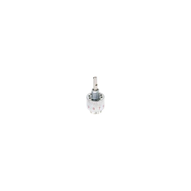
What is an R-2R Ladder DAC? (Binary-Weighted Resistor Ladder Basics)

R-2R Ladder DAC — TL;DR
An R-2R ladder DAC is a binary-weighted resistor network built from only two values—R and 2R—that turns digital codes into analog levels; because every stage repeats the same pair, ratio matching dominates accuracy and the structure scales cleanly with resolution. Each digital bit drives a switch that connects its branch either to the reference (Vref) or to ground; the branches sum at a single node to produce a proportional current (or voltage), which is then buffered to the output—also called an r 2r digital to analog converter. For small-batch builds, prioritize tight ratio matching over absolute tolerance, size the buffer or transimpedance amplifier for your load and bandwidth, decouple Vref locally, and use synchronous latching on code updates to reduce glitch energy on major-carry transitions.
Send your specs or BOM and get three safe options in 48 hours.
We’ll compare R-2R and suitable alternatives with indicative lead time and price range.
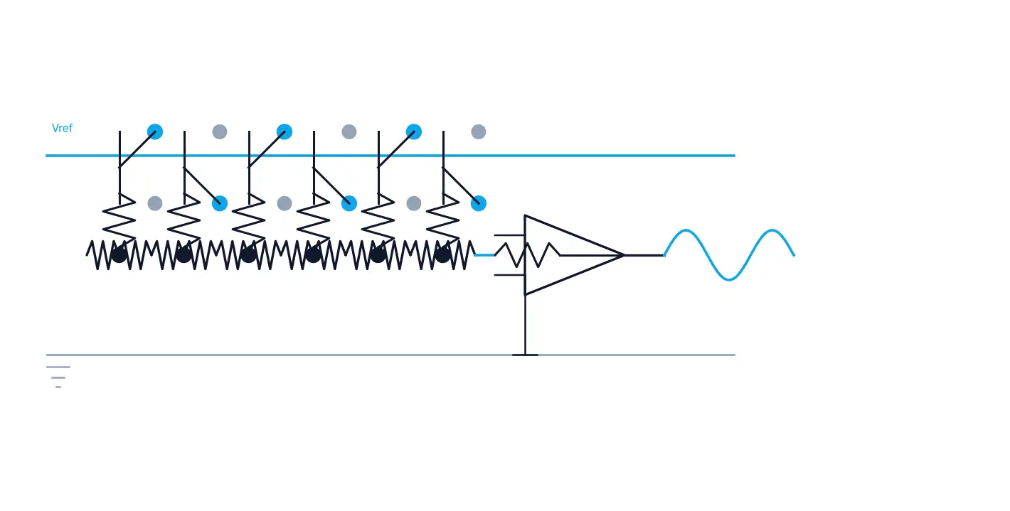
How the R-2R Ladder Works
Bit → Current/Voltage
In an R-2R ladder (a digital to analog converter resistor ladder), each digital bit drives a switch that connects its branch either to the reference source (Vref) or to ground. The network uses only two resistor values—R and 2R—so every branch contributes a binary-weighted share of current to a single summing node. With the most significant bit contributing roughly half of full-scale, and each lower bit halving again, the summed current (or, in a voltage-mode variant, the node voltage) is proportional to the code / 2N. That node is then buffered—typically by a transimpedance or voltage follower stage—so the load does not disturb the ladder’s weighting, and the output follows the code’s step pattern cleanly.
.png?x-oss-process=image/auto-orient,1/quality,q_70/format,webp)
Why only R and 2R
Using just two values simplifies sourcing and makes behavior repeatable across bits: ratios dominate accuracy in an R-2R ladder. Because every stage is built from the same R and 2R, matching between parts—rather than their absolute tolerance—sets linearity and monotonicity. For small-to-mid resolutions, tight ratio tracking from the same network or lot is far more valuable than chasing ultra-low absolute error on individual resistors. Thermal tracking also improves when elements share the same substrate or package, reducing drift-induced code bowing.
Output modes: current-mode vs. voltage-mode
- Current-mode (most common): the summing node behaves like a code-proportional current source and is held at virtual ground by a transimpedance/operational amplifier. Output impedance stays roughly constant (≈ R), and the op-amp converts current to voltage. Bandwidth and loop stability depend on the amplifier and the feedback network.
- Voltage-mode: the ladder’s end node develops a voltage directly; a low-impedance buffer then drives the load. Because the node voltage can sag with loading, buffering and consistent loading are important to preserve linearity.
Small-batch notes
- Reference drive: ensure Vref can supply the instantaneous code-dependent current; decouple locally (e.g., 10 µF ∥ 0.1 µF) and keep the return path short.
- Switch uniformity: MOSFET Ron matching and control timing affect DNL and glitch during major-carry transitions; consider synchronous latching.
- Quick checks: do a linear code sweep to inspect step uniformity, and a code histogram to spot missing codes or excessive jitter.
Matching, Accuracy & Monotonicity
LSB intuition: when matching is “good enough”
Treat 1 LSB ≈ FS/2N (FS: full-scale). If a branch’s relative error approaches ~1 LSB at the summing node, step widths become uneven—showing excessive DNL, potential missing codes, or loss of monotonicity (no code reversals). In an R-2R ladder, ratio matching between R and 2R dominates accuracy; absolute tolerance matters far less than how consistently each stage tracks the same ratio across temperature and time.

Experience ranges (engineering intuition, not hard limits)
- 8-bit: prefer ≤ 0.1–0.2% relative matching.
- 10-bit: prefer ≤ 0.05–0.1% relative matching.
- 12-bit: prefer ≤ 0.01–0.02%; consider thin-film networks, integrated arrays, or vendor-trimmed networks for tracking.
These are practical order-of-magnitude targets; the true budget depends on Vref quality, switch Ron matching, output loading, and temperature environment.
Temperature drift & tracking come first
Prefer resistor elements that track each other: same network, same lot, or the same substrate. Consistent temperature coefficients (TCR tracking) keep the R:2R ratio stable across warm-up and ambient swings. Layout and airflow should minimize temperature gradients along the ladder; tracking beats absolute precision for linearity and monotonicity.
Quick self-checks (bring-up)
- Linear code sweep: 0 → FS; steps should look uniform. Watch for abnormally wide or narrow steps.
- Code histogram: hold a stable input and tally output codes to spot missing codes or jitter-spread.
- A/B swap: replace a suspect branch with a well-matched pair and repeat; changes reveal local mismatch.

Dynamic Behavior & Glitch
Synchronous switching reduces glitch energy
Major-carry transitions (e.g., 01111111 → 10000000) flip several bits at once; real switches do not move simultaneously, so transient currents and charge injection produce a visible glitch. Use synchronous latching so all bits update on the same clock edge, and consider segmented (thermometer + R-2R) coding for the upper bits to equalize switching. Clean Vref decoupling and tight return paths further limit spike energy.
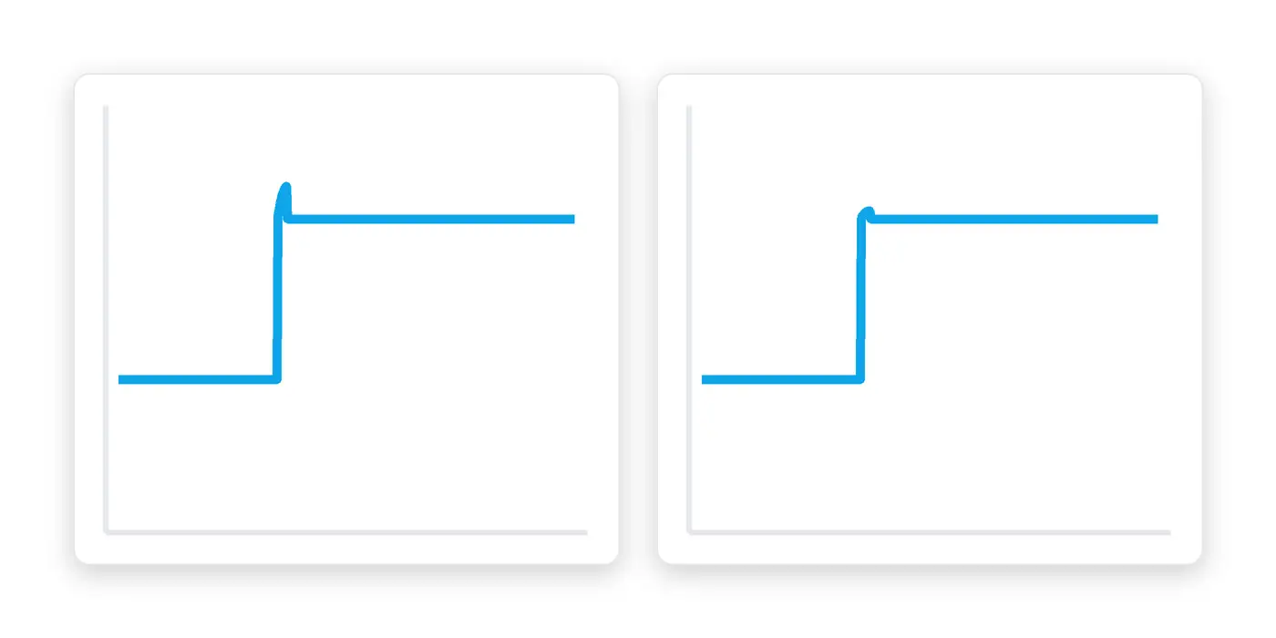
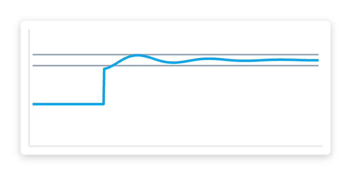
Settling time & loop stability
“Settling time” is the time to reach and remain within a chosen error band after a code step. It depends on switch symmetry and charge injection, amplifier GBW/slew/phase margin, feedback impedance, and capacitive loading. Choose switches with similar rise/fall behavior and amps that are stable with your transimpedance/voltage-follower network; verify stability on the actual PCB, not just in a socket or breadboard.
Filtering & bandwidth trade-offs
If the downstream path provides low-pass filtering (e.g., audio reconstruction or sensor smoothing), part of the glitch energy can be attenuated—balance cutoff, group delay, and stability. If your target is high speed with minimal glitch, evaluate a Current-Steering DAC architecture, which switches matched current sources rather than re-weighting through the ladder.
Reference, Buffer & Output Load
Reference drive (Vref)
An R-2R ladder presents a nearly constant load to the reference pin, yet code transitions still demand instantaneous current. Use a quiet source with local decoupling at the reference node: 10 µF ∥ 0.1 µF (place the small capacitor as close as possible to the pin; choose low-ESR for the bulk part). Keep the return path short and converge analog and digital grounds at a single point; a Kelvin connection to the reference pin improves stability. If digital noise bleeds into the reference rail, a small series bead or resistor can isolate it without adding excessive impedance.

Amplifier choice (transimpedance or buffer)
Current-mode (TIA): size the feedback resistor near Rf ≈ VFS,out/IFS, then add Cf for stability (a practical starting point places the zero well below the loop crossover, e.g., around GBW/10). Verify the op-amp’s GBW, slew rate, phase margin, input noise, and output swing under your expected load. Voltage-mode (buffer): follow the ladder’s end node with a low-impedance, rail-to-rail output amplifier that has sufficient bandwidth and load drive. In either case, prefer devices with comfortable stability margins and input common-mode ranges that cover your node voltages.
Output compliance
For current-mode stages, the transimpedance output should not be forced near the rails; check the stability impact of output capacitance and feedback impedance. For voltage-mode, keep the downstream load high enough or add a post-buffer driver/RC isolator so the ladder’s node voltage and linearity do not sag. As a rule of thumb, ensure the combined reference, amplifier, and load noise stays well below ≈ 0.3 LSBrms when expressed at the output.

Small-batch pitfalls
- Long wires + breadboard capacitance cause ringing and overshoot that distort step responses.
- USB power noise pollutes Vref and clocks, visible as low-bit jitter; prefer a dedicated, filtered rail.
- Signal traces near fast digital edges inject spikes into the summing node; route and shield accordingly.
- No single-point ground lets code-dependent return currents modulate the ladder; converge grounds at one node.
Quick checks (10-minute bring-up)
- Measure Vref ripple: AC-couple and observe 1 kHz–1 MHz; code steps should not amplify ripple.
- Code step response: confirm settling within your error band without sustained ringing.
- Static code histogram: look for missing codes and excessive spread at a fixed input.
- Load step: toggle typical vs. worst-case load and check for stability and headroom.
Pros & Cons
When R-2R shines
- Simple, cost-friendly structure: only two resistor values (R and 2R); easy to source or swap with network arrays.
- Nearly constant output impedance (≈ R): predictable loading for the buffer/TIA and cleaner summing behavior.
- Great for mid-resolution / mid-speed: practical for ~8–12-bit with kHz to low-MHz update rates (order-of-magnitude guidance).
- Prototype-friendly: with good matching, clean Vref, and synchronous updates, it’s quick to bring up in small batches.

When to consider other architectures
- High resolution sensitivity: beyond ~12-bit, tight ratio matching and temperature tracking dominate DNL/INL; thin-film/integrated networks help, or consider Delta-Sigma (trading speed for resolution and noise shaping).
- High speed / low-glitch / high SFDR: major-carry transitions inject glitch energy; Current-Steering DACs (segmented/thermometer coding, matched current sources) are typically better.
- Harsh thermal or switch mismatch: poor Ron matching or TCR tracking amplifies DNL/INL and drift.
- Audio chains with reconstruction filtering: system-level filtering and noise shaping often favor Delta-Sigma implementations.

Quick chooser (30-second checklist)
- Target ≤ 12-bit and mid-speed updates → R-2R ✅
- Minimal glitch / high spectral purity → Current-Steering ✅
- Ultra-high resolution / low speed with easy reconstruction → Delta-Sigma ✅
- Cost & simplicity for small-batch builds → R-2R ✅
- Strong temp gradients / tight linearity guarantees → prefer integrated networks or switch architecture ✅
- Audio playback / capture chains → start with Digital Audio to Analog ✅
Examples in Practice
MCU waveform generator (8–10-bit)
A small MCU-driven R-2R ladder works well for 8–10-bit waveforms at kHz to low-MHz rates. Use a simple RC or two-pole low-pass to smooth steps, and buffer the ladder end node before routing to external loads. Latch bits synchronously to tame glitches, and keep Vref clean—USB rails often inject ripple into the lowest bits.
Quick check: sweep a code ramp through the filter; verify uniform settling and no audible stair-steps at your test frequency.
Source calibrator (10–12-bit)
For current/voltage source calibration, 10–12-bit R-2R ladders benefit from thin-film networks or integrated arrays for tight ratio tracking. Size the TIA (Rf, Cf) from full-scale current and stability needs, and Kelvin-sense the output. Warm up the assembly to thermal steady state before taking measurements to avoid drift-induced bias.
Quick check: run a linear code sweep and a code histogram to spot DNL or missing codes after warm-up.
Audio / low-frequency synth
R-2R can drive low-frequency or audio synthesis if glitches are clock-aligned and a proper reconstruction filter is used. When spectral purity or major-carry spikes dominate requirements, consider segmented or current-steering DACs; for ultra-high resolution at low speed, Delta-Sigma is often easier to integrate.
Quick check: step-test through the audio chain and measure residual spikes or THD+N across the band of interest.
FAQ
What is an R-2R ladder DAC?
R-2R vs. binary-weighted DAC — what’s different?
How strict does resistor matching need to be?
How do I reduce glitches in an R-2R ladder?
Current-mode or voltage-mode output — which should I choose?

Related Articles
- ·Memory Chips: Materials, Applications, Types, and On-Chip Memory Explained
- ·Memory Chip Complete Guide: Definition, Manufacturers, Shortage, Manufacturing Process and Working Principles
- ·Fiber Optic Switch Guide: Definition, Connection Methods, Cabling, Disconnection and FAQ
- ·Optical Fiber Transmitter and Receiver Guide
- ·ICD Driver, LCD Driver & LCD Panel Driver Board Guide
- ·Touch Screen Overlay Guide for Commercial & Industrial Applications
- ·Cold Cathode Fluorescent Lamp Guide
- ·Complete Buying Guide for LED Video Walls & Commercial LED Displays
- ·The Complete Guide to Diode Lasers
- ·LED Emitter Guide: Definition, Brightness, Beam Angle, Soldering, Flashlight Upgrade, IR Usage and Grounding


.png?x-oss-process=image/format,webp/resize,h_32)


