

STMicroelectronics
STF13NM60ND
Single FETs, MOSFETs

Not available to buy online? Want the lower wholesale price? Please Send RFQ to get best price, we will respond immediately


.png?x-oss-process=image/format,webp/resize,p_30)


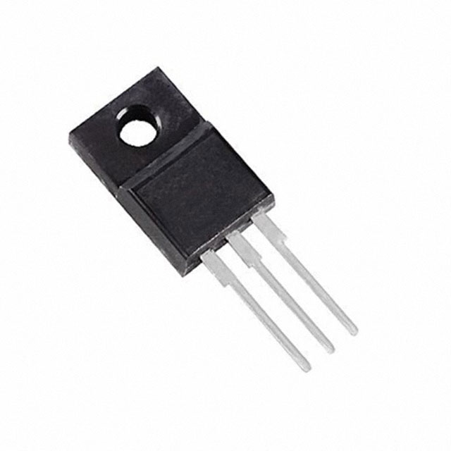
STF13NM60ND Description
STF13NM60ND Description
The STF13NM60ND is a high-performance N-Channel MOSFET from STMicroelectronics, designed for applications requiring high voltage and current handling capabilities. With a drain-to-source voltage of 600V and continuous drain current of 11A at 25°C, this device offers excellent performance in demanding power management applications.
STF13NM60ND Features
- High Voltage and Current Handling: STF13NM60ND can handle a drain-to-source voltage of 600V and a continuous drain current of 11A at 25°C, making it suitable for high-power applications.
- Low On-Resistance: The device has a maximum on-resistance of 380mOhm at 5.5A drain current and 10V gate-source voltage, contributing to high efficiency in power conversion.
- Low Gate Charge: With a maximum gate charge of 24.5nC at 10V gate-source voltage, STF13NM60ND reduces switching losses and improves overall efficiency.
- Robust Temperature Performance: Operating temperature range of -55°C to 150°C (TJ) ensures reliable performance in a wide range of environments.
- Compliance and Certifications: The device is compliant with RoHS3 and REACH standards, making it suitable for environmentally conscious applications.
- Package Type: Available in a through-hole TO220FP package, facilitating easy integration into existing designs.
STF13NM60ND Applications
The STF13NM60ND is ideal for a variety of high-power applications, including:
- Power Supplies: Its high voltage and current ratings make it suitable for use in power supply designs, particularly in applications requiring high efficiency and reliability.
- Motor Control: The low on-resistance and low gate charge of STF13NM60ND make it an excellent choice for motor control applications, where high efficiency and fast switching are critical.
- Industrial Automation: The device's robust temperature performance and high power handling capabilities make it suitable for use in industrial automation systems, where reliability and performance are paramount.
Conclusion of STF13NM60ND
The STF13NM60ND from STMicroelectronics is a high-performance N-Channel MOSFET that offers excellent voltage and current handling capabilities, making it an ideal choice for a variety of high-power applications. Its low on-resistance, low gate charge, and robust temperature performance contribute to high efficiency and reliability, while its compliance with RoHS3 and REACH standards make it suitable for environmentally conscious designs. With its high-performance characteristics and wide range of applications, the STF13NM60ND is a valuable addition to any power management or motor control design.
Tech Specifications
STF13NM60ND Documents
Download datasheets and manufacturer documentation for STF13NM60ND
STx13NM60ND Box Label Chg 28/Jul/2016 Related Parts


Shopping Guide


.png?x-oss-process=image/format,webp/resize,h_32)


©2025 ERSA Electronics Corporation.